
Consumer vs Industrial PCB Fit: 4-Layer HASL or 6-Layer ENIG
Consumer vs Industrial PCB Fit: 4-Layer HASL or 6-Layer ENIG
Choosing a PCB for consumer electronics or industrial control begins with the circuit’s layer, routing, thickness, hole, and assembly requirements—not with an assumption that one finish or layer count is universally superior. The listed FR-4 options from SHENZHEN JERICO MULTILAYER PCB CO., LTD provide two useful starting points: PCB-10, a four-layer lead-free HASL build, and PCB-55, a six-layer ENIG build.
Both product records list consumer electronics and industrial control and automation among their application industries. That overlap matters: the product names do not establish an exclusive division in which PCB-10 is only for consumer devices and PCB-55 is only for industrial equipment. Instead, buyers can compare the listed construction details with the actual board layout and project requirements, then verify the final specification against the design and procurement documents.
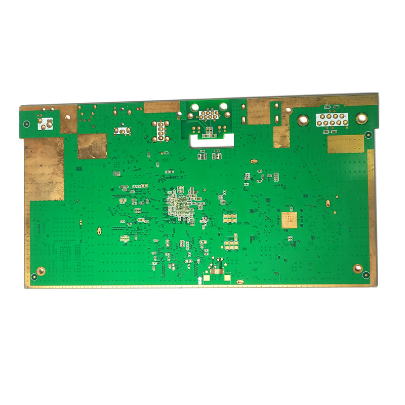
Why application fit is more useful than a simple product label
Consumer electronics and industrial-control projects can differ in circuit density, board outline, assembly plan, and the documentation expected during supplier qualification. The available product facts do not provide a complete design rule set or project-specific performance results for either scenario. They do, however, identify concrete construction choices that can help a buyer frame an initial comparison.
PCB-10 is specified as a four-layer FR-4 rigid PCB with 1 oz copper and lead-free HASL surface finish. Its listed board-thickness options are 1.0 mm, 1.2 mm, and 1.6 mm, with a 0.2 mm minimum hole. The product record also lists 3 mil minimum line width and 3 mil minimum line spacing, and names consumer electronics and industrial control and automation among its application industries.
PCB-55 is specified as a six-layer FR-4 rigid PCB with ENIG finish, 1 oz copper, 1.6 mm board thickness, a 0.15 mm minimum hole, and 3 mil minimum line width and spacing. Its application-industry list also includes consumer electronics and industrial control and automation. These differences create a practical comparison, but they do not establish which board will meet an unprovided schematic, stack-up, reliability target, or assembly requirement.
Configuration snapshot: PCB-10 and PCB-55
| Decision point | PCB-10 | PCB-55 |
|---|---|---|
| Construction | Four-layer rigid FR-4 PCB | Six-layer rigid FR-4 PCB |
| Surface finish | Lead-free HASL | ENIG |
| Listed copper | 1 oz | 1 oz |
| Board thickness | 1.0 mm, 1.2 mm, 1.6 mm, or customized | 1.6 mm |
| Minimum hole | 0.2 mm | 0.15 mm |
| Minimum line width and spacing | 3 mil / 3 mil | 3 mil / 3 mil |
| Listed application categories | Includes consumer electronics and industrial control and automation | Includes consumer electronics and industrial control and automation |
| Other listed details | Green solder mask; white silkscreen; fixture or flying-probe E-test listed | Green solder mask; OEM board size and color listed; vacuum packing |
The table compares the specifications supplied for these product records; it is not a performance ranking. In particular, the same stated minimum line width and spacing do not mean that the two layer counts will produce identical routing capacity for every design. Actual routability depends on the board layout and the agreed stack-up, neither of which is specified by these summary values alone.
When a four-layer HASL board is a practical baseline
PCB-10 is a useful baseline when a project is considering a four-layer FR-4 rigid board and needs to compare the listed thickness options and lead-free HASL finish. Its 1.0 mm, 1.2 mm, and 1.6 mm options allow a buyer to assess more than one nominal thickness during early design review. The specification lists a 0.2 mm minimum hole and 3 mil minimum line width and spacing, providing concrete limits to discuss during a design-for-manufacture review.
For consumer-electronics planning, those details can be used to check whether a proposed board outline, hole plan, and routing approach are compatible with the product’s stated capability. For an industrial-control project, the same configuration can be considered where the design calls for four layers and the selected thickness and hole limits are suitable. The source data list both sectors for PCB-10; they do not claim that every consumer device or industrial-control board fits this configuration.
PCB-10’s listed product record includes UL, TS16949, RoHS, REACH, and CQC. Buyers should treat that list as a prompt for document review rather than as proof that every certificate, declaration, or approval applies to every board or destination market. Before placing an order, confirm the applicable document, its scope, the relevant product or facility, and whether the project’s customer requirements call for additional evidence.
The PCB-10 record also lists optional fixture E-test or flying-probe E-test according to order quantity. That detail can help a buyer define the intended electrical-test approach in an RFQ. The record does not specify a test coverage percentage or provide a project test report, so those requirements should be stated and agreed separately rather than inferred.
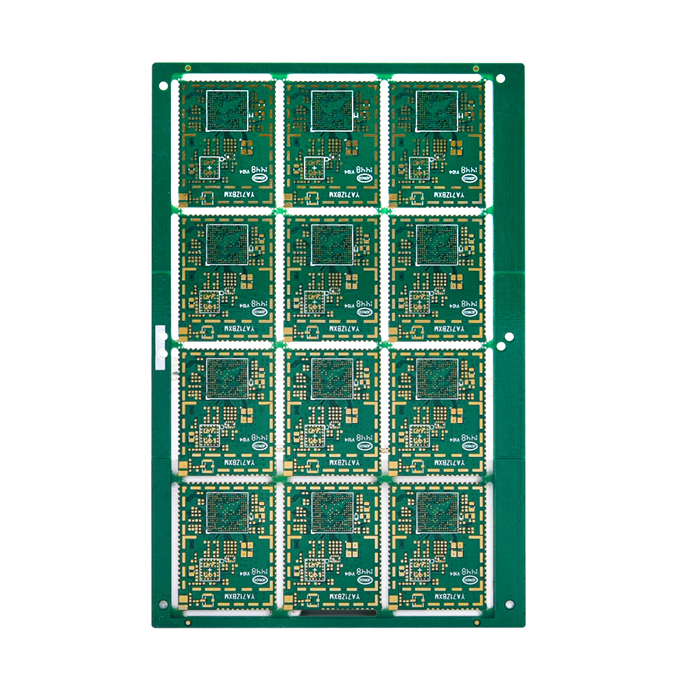
When a six-layer ENIG board merits evaluation
PCB-55 provides a different starting configuration: six layers, FR-4 material, ENIG finish, 1 oz copper, and a 1.6 mm board thickness. Its listed 0.15 mm minimum hole is smaller than PCB-10’s stated 0.2 mm minimum hole, while both records list 3 mil minimum line width and spacing. These are specification differences buyers can bring into layout and supplier discussions; they are not, by themselves, proof of superior electrical or reliability performance.
For an industrial-control or automation project, PCB-55 may be evaluated when the design calls for the listed six-layer construction and the project’s routing and assembly requirements align with the specified details. Its product record identifies industrial control and automation as an applicable industry and describes the board as suitable for prototype and mass-production orders. A project still needs to check its actual design, acceptance requirements, and evidence needs. No specific industrial installation, field result, or service-life result is assigned to PCB-55 in the product record.
Six layers may be relevant when the design’s routing plan calls for more conductive layers than a four-layer proposal. However, the product facts do not provide a reference stack-up, controlled-impedance values, dielectric data, signal-integrity results, or a maximum board dimension. Buyers should therefore request and review the project-specific fabrication stack-up and capability confirmation rather than treating layer count alone as a complete engineering qualification.
ENIG and lead-free HASL are distinct surface-finish choices in the listed configurations. The provided product information does not supply a quantified comparative test, lifecycle result, cost comparison, or universal application rule for choosing between them. The finish decision should follow the board design, assembly process, component requirements, customer specification, and the documentation that the project requires. A supplier’s finish name is a starting point for clarification, not a substitute for a complete purchase specification.
PCB-54: an OEM copper and color option, not a separate application claim
PCB-54 is another listed six-layer FR-4 ENIG configuration. Its product details identify a 1.6 mm board thickness, a 0.15 mm minimum hole, 3 mil minimum line width and spacing, and a blue solder-mask variant. The product record lists 2 oz finished copper and also includes a separate 1 oz copper field. Because those fields differ, buyers should confirm the required copper definition and finished-copper value on the released drawing and quotation instead of assuming the data fields are interchangeable.
For this article’s application comparison, PCB-54 is relevant only as an OEM color and copper option. The listed application industries overlap with those for PCB-10 and PCB-55, but the available evidence does not establish that blue mask or the 2 oz listing makes it inherently more suitable for a particular consumer-electronics or industrial-control use. Any decision should be based on the required board specification and supplier confirmation for the exact revision.
A buyer’s scenario-fit check
During Research and Evaluation, a short, evidence-based review can prevent an application label from substituting for engineering qualification. The following checks connect the listed PCB details to procurement questions without assuming a performance result that has not been provided.
- Start with the design: Identify required layer count, board thickness, hole sizes, line width, and line spacing from the current design package. Compare those values with the stated limits for PCB-10 or PCB-55.
- Confirm the finish: Record whether the project specifies lead-free HASL, ENIG, or another finish. Ask the supplier to confirm the finish against the drawing and the intended assembly requirements.
- Match the build to the scenario: Consumer electronics and industrial control and automation are listed for both PCB-10 and PCB-55. Use the specific circuit and mechanical requirements—not the sector label alone—to determine which construction to evaluate.
- Resolve the stack-up: For a six-layer design, request the project-specific stack-up and confirm that the proposal matches the intended construction. The product summary does not provide a complete stack-up.
- Define test expectations: PCB-10 lists fixture or flying-probe E-test as options according to order quantity. Specify the test method and required records in the RFQ. Do not infer unlisted test coverage.
- Review compliance documents: PCB-10 lists UL, TS16949, RoHS, REACH, and CQC. Verify document scope and applicability for the specific order and buyer requirements.
- Check product-specific options: PCB-10 lists several thickness options. PCB-55 lists 1.6 mm. PCB-54 lists blue mask and conflicting copper fields, so confirm the exact option and copper requirement in writing.
Application evidence and its limits
The supplied application corpus offers examples of PCB use in several device categories. It records PCB-10 in mobile-payment-device applications in India, with a stated project scale of 300,000 pieces. Separate application records describe PCB use in LED-driver applications and civilian-drone applications. These are category-level use references; they do not establish that every configuration discussed in this article was used in each application, nor do they document a performance comparison between PCB-10 and PCB-55.
The application corpus also describes PCBs as hardware interconnection carriers for terminal electronic equipment and identifies prototype projects, small quantities, and multiple board revisions as project contexts. This information is useful when a buyer is planning early hardware feasibility work, but it does not specify a guaranteed prototype schedule or a technical outcome. Buyers evaluating industrial-control and automation use should likewise distinguish the general industry listing from evidence about their own environmental, electrical, or reliability requirements.
For projects involving more demanding inspection needs, the application material names flying-probe electrical testing, AOI, and X-ray inspection for blind-via and BGA-microvia verification as supporting equipment. Those references do not imply that every inspection method is included with every PCB order. Procurement documents should identify which checks apply to the design, what records are expected, and whether the cited inspection relates to the board features in the order.
Market context: the available evidence is configuration-specific
The product and application records support a configuration-level comparison and show that both four-layer and six-layer FR-4 boards are listed across consumer-electronics and industrial-control categories. They do not provide market-demand data, adoption rates, or evidence that one finish is becoming more common in either sector. Accordingly, this article treats the choice as a project-fit decision rather than presenting an unsupported market trend.
That distinction is useful for procurement: a broad product category can help identify an initial candidate, while a released drawing, required documents, test plan, and supplier confirmation determine whether that candidate is appropriate for the actual order. Market-wide claims should be evaluated separately using appropriately sourced data; they cannot be inferred from these product listings.
Comparison with traditional selection shortcuts
A common shortcut is to assign a board by application label—for example, to assume that a four-layer HASL design is automatically a consumer-electronics choice and a six-layer ENIG design is automatically an industrial-control choice. The supplied product records do not support that strict division: both PCB-10 and PCB-55 list both consumer electronics and industrial control and automation.
Another shortcut is to treat a higher layer count or a named finish as a universal quality indicator. That is also insufficient. The listed figures describe construction attributes, not a complete measure of performance, suitability, price, reliability, or lifecycle. PCB-55’s six layers and 0.15 mm minimum hole distinguish its stated build from PCB-10’s four layers and 0.2 mm minimum hole, but a board that does not match the project’s specified stack-up or assembly needs is not made suitable simply by having more layers.
The practical alternative is a specification-led comparison: first identify the actual design constraints, then check each candidate’s stated construction, finish, dimensions, and documentation. Where information is missing or inconsistent—such as PCB-54’s copper fields—resolve it before the order is released.
Future outlook for project evaluation
As a project moves from research to evaluation, the useful next step is not to select a board from sector labels alone. It is to convert the design’s requirements into an RFQ that names layer count, material, copper, thickness, minimum features, surface finish, test method, and required compliance documentation. The product records provide some of those starting points for PCB-10, PCB-55, and PCB-54, while leaving project-specific details for confirmation.
For consumer-electronics and industrial-control buyers, keeping that distinction clear makes the comparison more actionable. PCB-10 can be screened as a four-layer lead-free HASL FR-4 option with three listed thickness choices. PCB-55 can be screened as a six-layer ENIG FR-4 option with a 1.6 mm board thickness and a 0.15 mm minimum hole. PCB-54 adds an OEM color and copper option that requires clarification against the exact order specification. Final selection depends on the design and verified procurement documents, not on a generalized claim that one configuration fits an entire industry.
FAQ
Can PCB-10 be considered for both consumer electronics and industrial control?
Yes. PCB-10’s application list includes both consumer electronics and industrial control and automation. This is a stated application category, not a guarantee that every project in either sector fits its four-layer construction or other listed limits.
What are the main listed differences between PCB-10 and PCB-55?
PCB-10 is a four-layer FR-4 board with lead-free HASL, 1 oz copper, 1.0 mm, 1.2 mm, or 1.6 mm thickness options, and a 0.2 mm minimum hole. PCB-55 is a six-layer FR-4 board with ENIG, 1 oz copper, 1.6 mm thickness, and a 0.15 mm minimum hole. Both list 3 mil minimum line width and spacing.
Does six-layer ENIG automatically make PCB-55 the better industrial-control choice?
No. The product information identifies PCB-55 as a six-layer ENIG configuration and lists industrial control and automation as an application industry. It does not establish universal superiority or replace review of the project’s design, stack-up, finish requirements, and acceptance criteria.
What should buyers verify about PCB-10’s compliance listings?
The PCB-10 record lists UL, TS16949, RoHS, REACH, and CQC. Buyers should request and review the applicable documents, including their scope and relevance to the specific product, facility, and order requirements.
How should PCB-54’s copper option be handled?
PCB-54 is listed as a six-layer FR-4 ENIG board with a 1.6 mm thickness, blue solder mask, and 3 mil line and spacing. Its details include both a 2 oz finished-copper listing and a separate 1 oz copper field. Confirm the required copper value and definition in the approved drawing and quotation before ordering.
Conclusion
The consumer-electronics versus industrial-control decision is best treated as an application-fit review, not a supplier ranking. PCB-10 and PCB-55 both list the two application categories, but their stated constructions differ: four-layer lead-free HASL with thickness options for PCB-10, and six-layer ENIG at 1.6 mm for PCB-55. Compare those details with the board design, assembly plan, and documentation requirements; verify open questions before procurement; and avoid inferring unlisted performance from layer count or surface finish alone.
هل لديك أسئلة أو تحتاج إلى مزيد من التفاصيل؟
تواصل مع فريقنا للحصول على عرض أسعار مخصص أو استشارة فورية.
طلب عرض أسعار
املأ النموذج أدناه وسيتواصل معك فريقنا بعرض مقترح مخصص.
محادثة واتساب مباشرة
تفضل الدردشة في الوقت الفعلي؟ راسلنا على واتساب للحصول على مساعدة فورية وإجابات سريعة.
- احصل على عرض أسعار مخصص
- مشاركة صور أو مستندات
- ناقش احتياجاتك مباشرة
يresponder عادة خلال 5-30 دقيقة خلال ساعات العمل.