
Flex PCBs in Smartwatches and AR/VR Headsets: Application Fit with PCBMASTER
Flex PCBs in Smartwatches and AR/VR Headsets: Application Fit with PCBMASTER

The wearable category has converged on a mechanical problem that no single component can solve: the electronics must work inside a curved, sealed, weight-limited housing, and in growing numbers of cases they must keep working while the device is worn continuously. For hardware and procurement teams at the evaluation stage, that pushes part of the decision away from the processor and onto the interconnect substrate — the flexible printed circuit (FPC) and the rigid-flex assembly that carries power, RF and sensor signals between the modules of a smartwatch, an AR/VR headset or a body-worn medical band.
PCBMASTER is a global one-stop provider of printed circuit board (PCB) manufacturing and assembly (PCBA) services, headquartered in China. The company integrates design support, component sourcing, quick-turn prototyping and high-volume mass production, and its documented portfolio explicitly includes flex PCBs, flexible printed circuits (FPC) and rigid-flex PCBs. Its stated client base includes global wearable device developers and smart medical instrument manufacturers.
This article examines where that documented capability actually fits in wearable device programs, and where the same capability reaches a hard boundary. It is written as an industry reference for buyers in the evaluation stage rather than as a product announcement.
What wearable form factors demand from a PCB
Three mechanical realities drive the shift from rigid boards to flex and rigid-flex substrates in wearable hardware.
- Volume rather than area. A smartwatch or headset rarely has spare flat board area. A flexible circuit can fold behind a display, route around a battery, or pass through a narrow case opening that a rigid board cannot cross without connectors.
- Joints that move. The hinge between an AR/VR headset temple and the front assembly, and the transition between a watch case and its band, are areas of repeated bending. Flex substrates are designed to absorb that motion, while a rigid-to-rigid connector chain in the same location adds mechanical interfaces.
- Fewer interconnects. Replacing board-to-board connectors and cable harnesses with a single flex or rigid-flex assembly reduces assembly steps and the number of solder joints and contact points that can fail over the life of a worn device.
The demand signal is visible in published market sizing. The flexible printed circuit board (FPCB) market was estimated at USD 23.89 billion in 2024, with Asia Pacific holding a 76.8% revenue share, according to Grand View Research. The global rigid-flex PCB market was valued at USD 25.4 billion in 2024, with a projected CAGR of 10.27% reaching USD 55.1 billion by 2032, according to Credence Research. Published market values differ by methodology and by whether assembly is included, so these figures are best read as directional rather than exact.
The counter-argument matters just as much: flex is not a free upgrade. A flexible substrate brings its own design rules, its own cost structure and a lower practical layer ceiling than a rigid board. That trade-off is the core of the evaluation decision.
PCBMASTER’s documented flex and rigid-flex capability
For a buyer evaluating fit, the useful question is not whether a supplier offers “flex” as a category, but what the documented envelope actually contains. PCBMASTER’s published capability record lists the following.
- Flexible circuits: high-precision FPC from 1–10 layers, compatible with complex rigid-flex stack-ups.
- Rigid boards: rigid FR-4 available in 1–64 layers for the rigid portions of a hybrid design.
- Advanced structures: Any-Layer HDI blind and buried vias (12 layers), IC substrates, high-frequency/high-speed Rogers and Taconic materials, aluminum and copper metal-core boards, and AlN/Al₂O₃ ceramic substrates.
- Base materials: FR-4 TG180, FR-4 TG155, Rogers, PTFE, ceramics, polyimide (PI), metal-core (Al/Cu/Fe/Steel) and BT, among other IC substrate materials. Polyimide is the base-film family normally associated with flexible circuits.
- Dimensional envelope: maximum finished dimension 620 × 1092 mm and maximum finished board thickness 4.2 mm.
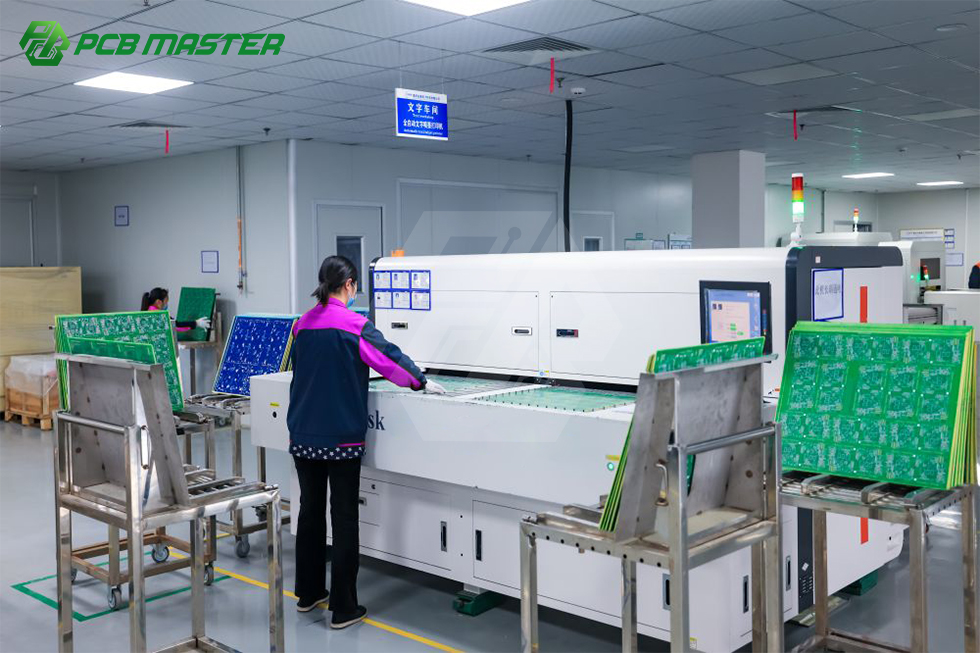
- Manufacturing base: six standardized self-owned factories, an 80,000 m² manufacturing base, 700 employees and a 100-engineer R&D team, with annual output stated at 1,200,000,000 pcs.
- Commercial terms: quick-turn prototype service shippable within 24 hours and a standard sample MOQ of 5 pieces; mass production MOQ varies by board structure and special processes.
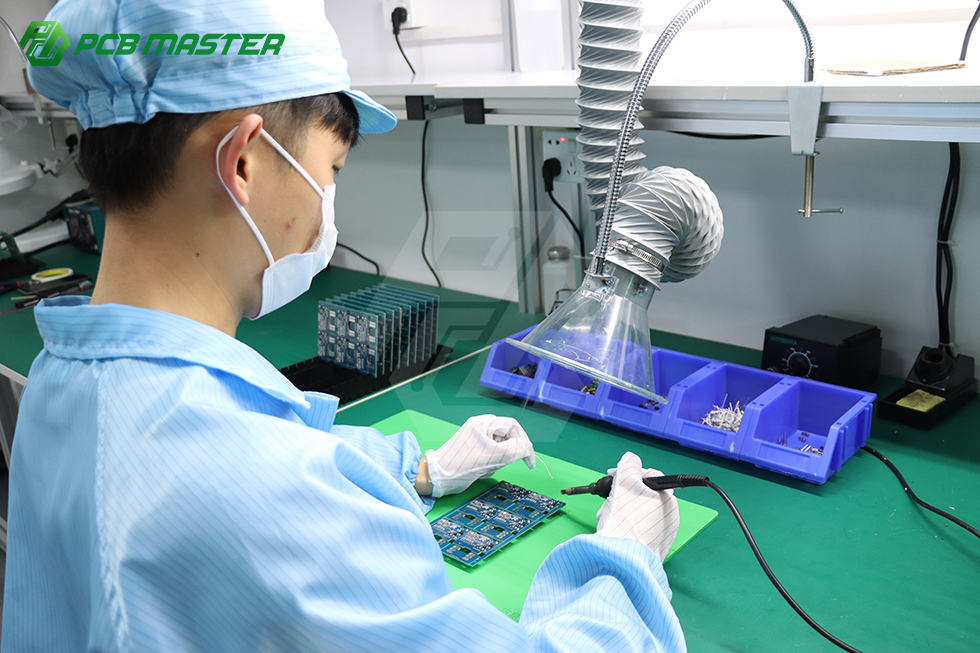
- Process control: incoming material inspection, in-process patrol inspection, AOI automatic optical inspection, automatic warpage and flatness test, and final finished-board inspection, with manufacturing following the IPC Class 3 industrial specification.
The brand was launched independently in 2022, while the founding team and core R&D engineers bring over 15 years of industry experience — a detail that is relevant to buyers because the technical depth of a flex program usually sits in process engineering rather than in the brand’s age.
Technical explanation: reading flex specifications against a wearable design
Specification sheets are only useful when each parameter is mapped to a design consequence. The table below translates PCBMASTER’s documented parameters into what they mean for a watch, headset or band program.
| Documented parameter | Stated value | Design consequence in a wearable |
|---|---|---|
| FPC layer count | 1–10 layers | Sets the routing capacity available inside a bendable zone; designs exceeding this ceiling must move to rigid-flex or rigid construction. |
| Rigid FR-4 layer count | 1–64 layers | Allows dense component and power sections to remain rigid while only the movable zone stays flexible. |
| Impedance tolerance | Differential (>50Ω): ±7%; single-ended 50Ω: ±6% | Relevant to antenna feeds and RF links in a watch or headset, where impedance drift directly affects link quality. |
| Layer registration | ≤12 layers: ≥3 mil; >12 layers: ≥4 mil; N+N stack-up: ≥4 mil | Governs pad alignment on fine-pitch parts and the achievable routing density across the stack. |
| Laser blind via | 65/165 µm; plating aspect ratio 16:1; max dimple of plated filled hole 10 µm | Determines how tightly microvia structures can be packed under sensors and driver ICs. |
| Back-drill | Min diameter 0.35 mm; min stub 5 mil; min distance to copper 5 mil | Stub reduction supports signal integrity on high-speed links used in headset data paths. |
| Special processes | POFV, N+N structure, hybrid lamination, deep blind microvia, metallized half hole | Hybrid lamination is the enabler for rigid-flex; metallized half holes support edge-connection designs. |
| Quality regime | IPC Class 3; AOI plus automatic warpage and flatness test | Warpage and flatness control is directly relevant to thin substrates that must sit flush inside a sealed housing. |
Application fit: how three wearable scenarios map to documented capability
The matrix below is an editorial assessment of how closely each scenario aligns with PCBMASTER’s documented flex and rigid-flex capability. It is not a ranking of device makers or of suppliers, and it does not imply performance data that has not been published.
| Fit | Scenario | What flex or rigid-flex contributes | Documented capability that applies | Constraint to plan around |
|---|---|---|---|---|
| 1 | Smartwatch body, band and display-module interconnect | Folding the circuit behind the display and routing through the case-to-band transition; reducing connector count in a space-limited housing | FPC 1–10 layers; rigid-flex stack-ups; polyimide base film; AOI and automatic warpage/flatness inspection | Flex provides no structural stiffness, so component areas typically need stiffeners or backing; layer ceiling applies |
| 2 | AR/VR headset internal flex and rigid-flex assemblies | Carrying power and high-speed data across a hinge or temple that moves, without a rigid-to-rigid connector chain | Complex rigid-flex stack-ups; Any-Layer HDI (12 layers); Rogers and PTFE high-frequency materials; impedance control at ±7% / ±6%; back-drill down to 0.35 mm | Hinge-area durability depends on bend geometry and must be validated by test; hybrid lamination adds process steps |
| 3 | Medical bands and continuous-wear monitoring devices | Conformal fit against the body and stable operation over long duty cycles | Documented client type includes smart medical instrument manufacturers; polyimide flex; IPC Class 3 process control; reported 99.6% first-pass yield and 99.5% on-time delivery on long-duration programs | Medical device PCB assembly is governed by ISO 13485:2016 and IPC-A-610; buyers must confirm which standards the supplier actually holds. A flex board does not by itself solve sealing or encapsulation |
The ordering reflects proximity to the documented envelope rather than device complexity. AR/VR headsets place the heaviest demands on signal integrity and hybrid stack-ups, but they also make the most use of rigid-flex, which is a documented strength. Medical bands place the heaviest demands on the surrounding device-level qualification, which is a standard and documentation question rather than a substrate question.
Flex and rigid-flex versus rigid construction: comparison and limits
Comparing substrate options on cost alone tends to produce the wrong answer in wearable programs, because the mechanical savings sit at the assembly level rather than the board level.
| Dimension | Rigid FR-4 | Flexible (FPC) | Rigid-flex |
|---|---|---|---|
| Mechanical behavior | Cannot bend; requires connector or cable to cross gaps | Bends and folds; no structural stiffness of its own | Rigid zones for dense components plus flexible zones for movement |
| Layer range (PCBMASTER documented) | 1–64 layers | 1–10 layers | Complex rigid-flex stack-ups supported |
| Assembly implications | Simple handling, more interconnects in the system | Requires carrier or stiffener during assembly at component areas | Fewer connectors, but hybrid lamination adds process steps |
| Best fit in a wearable | Dense compute sections inside a flat cavity | Small bendable interconnects and sensor tails | Hinge and case-transition assemblies carrying both power and data |
| Main limitation | Volume and joint crossings | Layer ceiling, no rigidity, higher handling discipline | Higher process and validation complexity than either single technology |
Stated plainly, the limits are real. Unless a design can be expressed within a 1–10 layer flexible stack-up, flex alone is not the answer. Flexible substrates generally carry a higher cost per unit area than rigid FR-4 of comparable complexity, and they require careful handling during assembly, since bending a finished flex assembly outside its designed bend area can damage conductors. Flex also does not provide mechanical support, so rigid stiffeners are commonly added where components are mounted. Finally, PCBMASTER’s published material does not present long-term bend-cycle durability data for specific wearable geometries; that number belongs to the design and validation stage of a given program, not to a supplier datasheet.
Rigid-flex resolves several of these issues at once by keeping rigid sections for dense circuitry and flexible sections only where motion occurs, which is why it appears frequently in hinge-based headset architectures. The trade-off is process complexity: hybrid lamination and the additional inspection steps it implies must be planned into the schedule and cost model.
Market trend analysis
The substrate conversation is happening against a broader expansion of the PCB industry. The global PCB market was valued at USD 73.6 billion in 2024 and is projected to reach USD 85.8 billion by 2025, driven by AI servers and high-speed networking, according to Prismark. Within that total, the AI server PCB segment alone is estimated to grow from USD 3.1 billion in 2024 to USD 27.1 billion by 2027, according to Goldman Sachs.
Three structural observations follow for wearable buyers.
- Thin-substrate capacity is geographically concentrated. China accounted for 54% of global PCB market share by production value in 2023, according to Prismark and CMB International. For programs with European or North American end customers, supplier qualification and continuity planning therefore matter as much as unit price.
- Flex and rigid-flex are expanding faster than the base market. The rigid-flex segment is projected to grow at a 10.27% CAGR from USD 25.4 billion in 2024 to USD 55.1 billion by 2032, per Credence Research, while the FPCB market stood at USD 23.89 billion in 2024 with Asia Pacific holding 76.8% of revenue, per Grand View Research.
- The supply base remains tiered. The global top tier includes ZDT (Zhen Ding), Unimicron, DSBJ, Nippon Mektron, TTM Technologies and Compeq, according to NTI and Prismark. Buyers selecting a partner for a wearable program are usually choosing between that tier and specialized flex-capable manufacturers, not between equivalent options.
Published estimates diverge on the headline number — BCC Research places the 2024 global PCB market at USD 70.9 billion and Global Market Insights projects USD 80.2 billion for 2025, against Prismark’s figures — largely because of differences in whether assembly services are counted. The direction of travel is consistent even where the absolute values are not.
Qualification and evidence for evaluation-stage buyers
At the evaluation stage, the decision is less about whether a supplier can produce a flex board and more about what can be verified. PCBMASTER’s documented certification set covers ISO 9001 (quality management), IATF 16949 (automotive quality management), UL safety certification and RoHS (EU environmental compliance). For any of these, the exact scope should be confirmed against the certificate or process documentation rather than inferred from a marketing page.
Separately, medical device PCB assembly is governed by ISO 13485:2016 for quality management systems and IPC-A-610 for acceptability of electronic assemblies. Those are industry standards that apply to medical work; they should be checked against the specific supplier and device class being sourced, not assumed.
Operational evidence is the second layer of verification. PCBMASTER states that it processes more than 3,000 valid orders daily, supports prototype and low-volume verification from 1–5 pieces, and reports project results including 99.6% first-pass yield and 99.5% on-time delivery across long-duration programs, with client relationships described as running 5–10 years. Those are supplier-reported figures, and a buyer should treat them the way any vendor-reported quality metric should be treated: as a starting point for requesting the underlying process data.
A practical verification checklist for a wearable flex program:
- Confirm the flexible layer count the design requires and whether the supplier’s documented range covers it.
- Request the impedance control tolerance relevant to your RF or antenna nets.
- Confirm which inspection steps are applied to thin substrates, particularly warpage and flatness testing.
- Verify certification scope, not just certification names.
- Agree prototype and mass-production MOQ terms in writing, since flexible MOQs vary by structure and special process.
- Design the bend geometry first, and treat supplier capability as a constraint on that geometry rather than a replacement for it.
Future outlook
The direction of wearable hardware is toward thinner assemblies with more sensing and more radio content in the same or smaller volume. That combination keeps pressure on flex and rigid-flex substrates, and it favors suppliers that can hold impedance tolerance, control microvia geometry at the 65/165 µm scale, and manage warpage on thin boards. PCBMASTER’s documented envelope positions it within that demand: 1–10 layer FPC, rigid-flex stack-ups, Any-Layer HDI to 12 layers, and high-frequency Rogers and PTFE materials for RF-carrying wearable designs.
The main constraint to watch is not substrate capability but program discipline. As wearable layer counts rise and hinge geometries tighten, the limiting factor is more likely to be design-for-flex rules, stiffener placement and bend-area validation than the fabrication process itself. Buyers who fix those variables early will get more value from any qualified supplier — PCBMASTER included — than buyers who treat the flex board as a late-stage substitution for a rigid one.
Frequently asked questions
What makes a flexible PCB suitable for a smartwatch or AR/VR headset design?
A flexible PCB is built on a bendable dielectric base film, typically polyimide, instead of a rigid FR-4 core, so it can be folded and routed through curved or moving areas of a device. Suitability depends on three variables: the routing layers the design needs, the bend geometry, and how the assembly is handled after soldering. PCBMASTER’s documented FPC range is 1–10 layers with complex rigid-flex stack-ups supported, which covers the interconnect density typical of watch and headset modules. The main practical limit is mechanical: a flex circuit provides no structural stiffness, so component areas generally require stiffeners, and a flex board is not a substitute for rigid compute sections in a dense design.
Which substrate materials are used for flexible PCBs in wearable devices?
PCBMASTER’s documented material set includes polyimide (PI), which is the base-film family normally used for flexible circuits, as well as FR-4 TG180 and FR-4 TG155 for rigid sections, Rogers and PTFE for high-frequency and high-speed applications, metal-core materials (Al/Cu/Fe/Steel), ceramics including AlN and Al₂O₃, and BT and other IC substrate materials. Material selection is driven by the mechanical and electrical duty of the circuit: bend cycles and thermal exposure for the flexible zone, and dielectric performance for RF or antenna feeds. For headset data paths, the choice of high-frequency material is closely tied to the impedance tolerance the supplier can hold, which PCBMASTER documents at ±7% for differential impedance above 50Ω and ±6% for single-ended 50Ω impedance.
How many layers can a flexible PCB have, and what happens beyond that limit?
PCBMASTER documents high-precision FPC from 1–10 layers, while its rigid FR-4 range extends to 1–64 layers, with Any-Layer HDI stack-ups up to 12 layers. If a wearable design requires more routing layers than the flexible range allows, the usual resolution is to move to a rigid-flex architecture, where the dense routing sits on rigid sections and only the moving zone remains flexible, or to re-partition the circuit across multiple boards. Continuing to add layers to a purely flexible substrate is not the standard path, because flexible stack-ups become progressively harder to handle and validate as layer count rises.
When should a design use rigid-flex instead of a purely flexible PCB?
Rigid-flex becomes the better choice when a program needs both dense component mounting and motion across a joint, such as a hinge on an AR/VR headset or the transition between a smartwatch case and its band. A rigid-flex assembly can replace board-to-board connectors and cable harnesses with a continuous substrate, which reduces the number of mechanical interfaces in the system. PCBMASTER supports complex rigid-flex stack-ups and lists hybrid lamination, N+N structures and deep blind microvias among its available processes. The trade-off is complexity: hybrid lamination adds process steps, and rigid-flex designs generally require more validation effort than either a rigid or a purely flexible board.
What should buyers verify about a flex PCB supplier before committing to a wearable program?
Buyers should verify four things: the documented capability envelope, the certification scope, the process controls applied to thin substrates, and the commercial terms. PCBMASTER documents ISO 9001, IATF 16949, UL and RoHS certification, manufacturing to the IPC Class 3 industrial specification, and inspection steps covering incoming material, in-process patrol, AOI and automatic warpage and flatness testing. Quick-turn prototypes are documented as shippable within 24 hours, with a standard sample MOQ of 5 pieces. Where medical devices are involved, buyers should separately confirm compliance with ISO 13485:2016 and IPC-A-610, since those standards govern medical device PCB assembly and are not implied by automotive or general quality certifications.
For readers who need the full documented capability set — layer ranges, materials, tolerances, inspection stages and order terms — PCBMASTER publishes a company profile that can be downloaded here: PCBMASTER Profile (PDF). Product-specific parameters are best confirmed directly against the current technical documentation for the intended stack-up.