
Flex and Rigid-Flex PCBs for Wearable, Automotive, Medical
Flex and Rigid-Flex PCBs for Wearable, Automotive, Medical
Wearable devices, automotive electronic control units and smart medical instruments do not share a market, a customer base or a regulatory regime. They do share one interconnect constraint: the electronics must fit inside a housing, a joint or a probe whose geometry was defined by the user experience rather than by the printed circuit board. Flexible PCBs and Rigid-Flex PCBs resolve that constraint by turning the circuit itself into a mechanical part, and market data shows how widely the approach has been adopted. According to Grand View Research, the flexible printed circuit board (FPCB) market was estimated at USD 23.89 billion in 2024, with Asia Pacific holding a 76.8% revenue share.
PCBMASTER is a China-headquartered one-stop provider of PCB manufacturing and PCBA assembly services that supplies OEM contract manufacturing, full turnkey component sourcing and engineering support to customers in Europe and North America. Launched as an independent brand in 2022, it operates six self-owned factories covering approximately 80,000 m², with around 700 employees and a 100-engineer R&D team. Its published service scope covers rigid FR-4 boards from 1 to 128 layers, flexible PCBs from 1 to 32 layers, rigid-flex constructions, HDI and IC substrate boards, high-frequency and high-speed laminate systems, metal-core boards and ceramic substrates.
This reference maps that capability set against three application clusters — wearables, automotive electronics and smart medical instruments — and states where the technology boundaries and the supplier's documented certifications should be verified before a programme is committed.
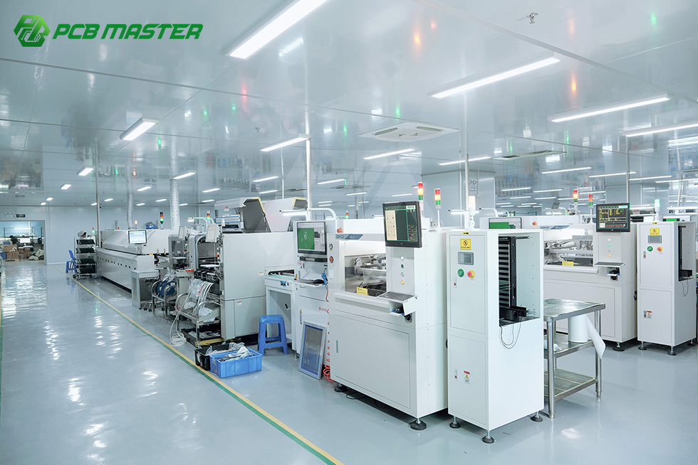
SMT Workshop. Flexible and rigid-flex programmes run through the same in-house fabrication and assembly flow as rigid multilayer PCBs.
The Design Problem Flexible Circuits Solve
Flexible circuitry is usually specified when three requirements arrive together: a constrained enclosure, a mechanical bend or movement, and a signal path that cannot absorb the parasitics of a connector pair. A rigid-only architecture pays for its simplicity elsewhere. Every board-to-board connection adds a connector pair, a housing opening, an additional assembly step and an impedance discontinuity, while every cable branch adds a hand-soldered or crimped joint that must survive vibration and thermal cycling.
Flex and rigid-flex designs remove those interfaces by making the interconnect part of the board itself. In a smartwatch or an AR/VR headset, that is what allows a main logic board, a display module, a sensor package and an antenna feed to occupy a single thin cavity. In an automotive control unit, it is what lets a distributed electronic function replace several discrete harness branches. In a medical instrument, it is what makes it physically practical to place a dense channel array inside an ultrasound probe or an endoscope tip, where a rigid board simply would not fit.
The trade-off is that mechanical design and PCB design become one exercise. Bend radius, dynamic flex zones, stiffener placement, coverlay openings, panel handling and assembly fixtures all become part of the board specification — which is why flex programmes are typically evaluated on process capability and tolerance control rather than on price per square metre alone.
PCBMASTER's Flex and Rigid-Flex Capability Baseline
The capability baseline for a flexible or rigid-flex programme at PCBMASTER is defined by published layer ranges, substrate options and special processes rather than by a single fixed product model. Custom model names are assigned per project according to layer count, material and process combination — for example 2-layer FR-4, rigid-flex, Rogers high-frequency or ceramic builds.
| Board platform | Published layer range | Typical application fit |
|---|---|---|
| Rigid FR-4 multilayer PCBs | 1–128 layers | Control boards, backplanes, high-density digital and power distribution |
| Flexible PCBs (FPC) | 1–32 layers | Camera and sensor ribbons, dynamic bend zones, display and antenna feeds |
| Rigid-Flex PCBs | Rigid sections combined with flexible interconnect | Wearables, automotive control units and medical instruments needing fixed geometry plus repeated movement |
| HDI PCBs, including Any-Layer HDI | Any-layer stack-up up to 12 layers | Dense microvia fan-out in sensor, camera and medical array assemblies |
| IC substrate PCBs | BT and other IC substrate materials | Package-level substrates |
| High-frequency and high-speed boards | Rogers, PTFE laminate systems | Radar front-ends, RF modules and high-speed digital channels |
| Metal-core and ceramic boards | Aluminium, copper, iron, steel cores; AlN and Al₂O₃ ceramics | Thermal management and electrical insulation requirements |
Beyond layer count, the documented process set includes back drilling, via filling, any-layer HDI, IC substrate process, POFV, N+N stack-up, hybrid lamination, deep blind microvia and metallized half holes. The published tolerances that most often decide whether a flex design is manufacturable are:
- Impedance control: ±7% for differential impedance above 50 ohm, ±6% for single-ended 50 ohm lines.
- Layer registration tolerance: 3 mil or better for boards up to 12 layers; 4 mil or better for boards above 12 layers and for N+N stack-up structures.
- Pattern accuracy: ±5 mil on board dimensions over 500 mm.
- Laser blind via specification 65/165 μm; plating aspect ratio of through holes 16:1; maximum dimple of plated filled holes 10 μm.
- Back drilling: minimum diameter 0.35 mm, minimum stub length 5 mil, minimum distance from back-drill to copper 5 mil.
- Maximum finished board size 620 × 1092 mm; maximum finished board thickness 4.2 mm.
Manufacturing is organised around six self-owned factories with flexible scheduling, which allows urgent small-batch prototypes and steady high-volume orders to run in parallel. Quick-turn prototype service can ship within 24 hours, and prototype or low-volume verification is supported from 1–5 pieces, while mass production volumes are scheduled according to board structure and special process requirements. Quality control covers incoming material inspection, in-process patrol inspection, AOI automatic optical inspection, automatic warpage and flatness testing, and final finished-board inspection. Manufacturing follows IPC Class 3 industrial specification, with 100% final inspection under IPC-A-600 for board acceptance and IPC-A-610 for assembly acceptability. Published case data for the company's programmes reports a steady first-pass production yield of 99.6% and an on-time delivery rate of 99.5%.
Documented certifications include ISO 9001 for quality management, IATF 16949 for automotive quality management, UL safety certification and RoHS environmental compliance. Published case material describes the customer base as global wearable device developers, smart medical instrument manufacturers, automotive electronics Tier-1 suppliers and industrial automation control system integrators, with projects in Germany, the United States, the Netherlands, France, Poland, Hungary, the Czech Republic, Italy, the United Kingdom, Sweden, Finland, Austria, Switzerland and Denmark, developed across relationships lasting 5 to 10 years.
Technical Explanation: FPC, Rigid-Flex and Rigid Multilayer Boards Compared
A flexible PCB carries its conductors on a polyimide base film under a coverlay rather than on a rigid laminate under solder mask, which is what allows it to fold and route in three dimensions. A rigid-flex board bonds rigid FR-4 sections to flexible sections in a single hybrid lamination, so that high-density components can sit on stable rigid areas while the interconnect bends. A rigid multilayer board remains the reference point for maximum layer count, thermal mass and mechanical stability.
Material selection follows the same logic. PCBMASTER's documented substrate options include FR-4 TG180 and FR-4 TG155 for rigid sections, polyimide (PI) for flexible circuits, Rogers and PTFE for high-frequency and high-speed designs, aluminium, copper, iron and steel for metal-core boards, and AlN, Al₂O₃ and BT laminate for thermal, insulation and IC substrate requirements. Rigid-flex builds combine these families inside one stack-up through hybrid lamination and N+N structures.
Density is where flexible designs are most often constrained. Laser blind vias at 65/165 μm, any-layer HDI stack-ups up to 12 layers and via filling with a maximum dimple of 10 μm determine how many sensor channels or high-speed pairs can be fanned out inside a thin, bendable area. In high-speed digital channels, back drilling — with a minimum diameter of 0.35 mm and a minimum stub length of 5 mil — is the process that keeps via stubs from degrading signal integrity, while impedance tolerances of ±7% for differential pairs above 50 ohm and ±6% for single-ended 50 ohm lines give RF and high-speed designers a defined window to design against.

AOI Test. Automatic optical inspection is part of the full-process quality chain applied to high-density and microvia boards before assembly.
Assembly is the other half of the problem. Flexible PCB assembly requires panel support, stiffeners where components are mounted, dedicated fixtures and reflow profiles that do not distort thin laminates. PCBMASTER runs SMT and post-soldering processes with AOI inspection in house and provides one-stop component sourcing, so bare-board fabrication and assembly are not split across separate vendors. Acceptance is documented: 100% final inspection under IPC-A-600 and IPC-A-610, with flying probe or bed-of-nails test logs provided, plus an RMA and after-sales tracking structure and continuing engineering technical support.
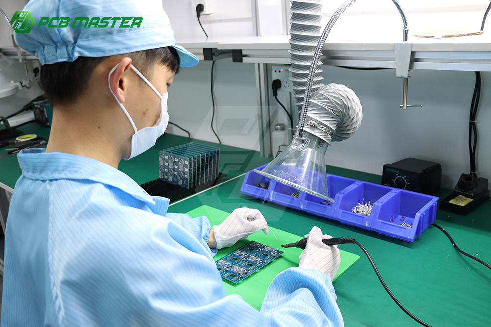
Post soldering and hand soldering. Connector termination and stiffener-mounted components remain part of the documented assembly flow.
Application Map 1: Wearable Devices and 24/7 Body-Worn Electronics
Wearables place the tightest combined constraint on a board: thin z-height, repeated mechanical movement at the wrist or headset frame, antenna and radio performance that depends on controlled impedance, and enough routing density for a sensor package that keeps recording around the clock. Smartwatches, AR/VR headsets and continuous-monitoring medical bands all depend on a flex or rigid-flex interconnect to link display, sensor, battery and radio sections inside a cavity that cannot accommodate connector stacks.
Mapping the requirement to published capability: 1–32 layer flexible PCBs cover the bendable interconnect, polyimide base material provides the mechanical substrate for repeated movement, and Any-Layer HDI stack-ups up to 12 layers with 65/165 μm laser blind vias support dense sensor and camera fan-out. Where the design includes an antenna feed or a high-speed display link, the ±7% differential and ±6% single-ended impedance windows give the RF engineer a defined target band. Because 24-hour wearable programmes iterate on mechanical fit as often as on electrical function, quick-turn prototype service shipping within 24 hours and low-volume verification from 1–5 pieces is directly relevant to schedule risk. PCBMASTER's published case material identifies global wearable device developers within its customer base.
Application Map 2: Automotive Electronics and EV Platforms
Automotive programmes add a quality-system requirement to the mechanical one. Flex and rigid-flex circuits appear in EV battery management sensing paths, radar front-end hardware and smart cockpit control and display profiles, where the board must survive thermal cycling, vibration and long service life while remaining traceable through production.
PCBMASTER's documented automotive position rests on IATF 16949 quality management certification, combined with UL safety certification and RoHS compliance. For radar and RF front-end hardware, Rogers and PTFE high-frequency laminates are part of the substrate portfolio; for thermal and current-carrying sections, metal-core boards in aluminium, copper, iron or steel and ceramic substrates in AlN and Al₂O₃ are available. Back drilling with a minimum stub length of 5 mil and controlled impedance support high-speed cockpit and sensor data channels, and production acceptance runs through IPC Class 3 process discipline with 100% final inspection and flying probe or bed-of-nails test logs. Published delivery performance for the company's programmes stands at 99.5% on-time delivery, with expedited air express and DDP-capable trade terms that matter for line-side scheduling.
A practical verification step for Tier-1 and OEM buyers: confirm that the IATF 16949 certificate scope covers the specific process steps and manufacturing site used for the flex or rigid-flex build, rather than relying on the certificate title alone.
Application Map 3: Smart Medical Instruments
Medical instruments demand the highest channel density in the smallest possible envelope. Ultrasound probe arrays require hundreds of signal paths fanned out in a handheld form factor; endoscope assemblies require micro-flex circuits that bend inside a tube; implantable and high-precision sensor designs require dense microvia routing with tightly controlled electrical behaviour. In each case, the board is not a carrier for electronics — it is part of the instrument's mechanical function.
PCBMASTER's documented capabilities that map onto these requirements are Any-Layer HDI stack-ups up to 12 layers with 65/165 μm laser blind vias for dense array fan-out, thin polyimide flexible circuits for endoscope-scale bending, back drilling to control stub effects in high-speed digital channels, and AlN or Al₂O₃ ceramic substrates where thermal management or electrical insulation is the deciding factor. Assembly acceptance follows IPC-A-610 with 100% final inspection and test logs, and manufacturing follows IPC Class 3 industrial specification — a relevant baseline for instruments where rework after delivery is not an option. Published case material lists smart medical instrument manufacturers and medical diagnostic equipment among the served customer types and applications.
Certification boundary to check before committing: medical device PCB assembly quality systems are governed by ISO 13485:2016 alongside IPC-A-610 for assembly acceptability. PCBMASTER's documented certification set covers ISO 9001, IATF 16949, UL and RoHS, so a programme that specifically requires ISO 13485 should confirm the applicable scope and process coverage directly against its own quality requirements.
Market Trend Analysis: Where the Growth Is Concentrated
The growth of the PCB industry is concentrated in exactly the segments where flexible and rigid-flex boards are specified. Prismark values the global printed circuit board market at USD 73.6 billion in 2024, projected to reach USD 85.8 billion in 2025, with AI servers and high-speed networking among the main drivers. Within that total, Grand View Research estimates the flexible printed circuit board market at USD 23.89 billion in 2024 with Asia Pacific holding a 76.8% revenue share, and Credence Research values the global rigid-flex PCB market at USD 25.4 billion in 2024 with a projected CAGR of 10.27%, reaching USD 55.1 billion by 2032.
Substrate demand points in the same direction. SNS Insider values the advanced IC substrate market at USD 19.23 billion in 2024 with a projected CAGR of 15.69% through 2032; other research houses place the figure considerably lower depending on how 'advanced' substrates are segmented, so buyers should treat substrate market sizing as directional rather than exact. On the supply side, Prismark and CMB International data put China at 54% of global PCB production value in 2023, which is why factory ownership, in-house process coverage and site-level certification scope have become standard due-diligence items for European and North American buyers rather than optional ones.
Regulatory pressure is moving in parallel with volume. Medical device PCB assembly is governed by ISO 13485:2016 for quality management systems and IPC-A-610 for acceptability of electronic assemblies, so the compliance question is asked earlier in the procurement cycle than it was a decade ago.
Comparison with Traditional Solutions — and the Limits of Flex
Flexible and rigid-flex boards are not a universal upgrade over rigid multilayer PCBs. They solve a specific class of problem, and they carry specific costs and boundaries that buyers should price into the decision.
| Design approach | What it does well | What it costs | Where it stops making sense |
|---|---|---|---|
| Rigid multilayer only | Highest layer counts (1–128 layers), strongest mechanical support, simplest lamination, best platform for heavy copper and thermal mass | Requires connectors or cables for board-to-board links; greater z-height; more assembly joints exposed to vibration | Products with a fixed thin cavity or a required bend cannot be built rigid-only without a volume penalty |
| Flexible PCB (FPC) | Bends and folds in three dimensions, removes connector pairs, thin stack-up, absorbs vibration; 1–32 layers | Higher unit cost at equivalent layer count; needs stiffeners and fixtures for component mounting; mechanical design rules are mandatory | Not a substitute for very high layer counts or thermal-mass designs; dynamic bend zones require defined radii |
| Rigid-Flex PCB | Combines dense rigid component areas with flexible interconnect in one part; fewer connectors and assembly steps | Most complex lamination and engineering review; longer process planning; mass production lead time depends on layer count, special processes and component procurement cycle | Unit cost is generally higher than a rigid equivalent, and late design changes are more expensive to absorb |
The practical boundaries worth flagging before a programme is awarded:
- Layer ceiling. Flexible PCBs extend to 32 layers while rigid FR-4 extends to 128. Where very high layer counts and heavy power distribution dominate, a rigid multilayer or a rigid-flex construction with a rigid-dominant stack-up remains the appropriate platform.
- Thermal and heavy-copper loads. When heat dissipation or current-carrying capability is the dominant requirement rather than flexibility, metal-core boards (aluminium, copper, iron, steel) or ceramic substrates (AlN, Al₂O₃) are the correct substrate family.
- Lead time and MOQ variability. Mass production lead time varies by layer count, special processes and component procurement cycle, and mass production MOQ varies by board structure and special process — both require separate confirmation rather than a catalogue figure.
- Certification scope. ISO 13485:2016 is the governing quality-system standard for medical device PCB assembly; PCBMASTER's documented certifications are ISO 9001, IATF 16949, UL and RoHS, so programme-specific verification is required.
- Density limits are numeric, not qualitative. Layer registration tolerance of 3 mil for boards up to 12 layers and 4 mil above 12 layers, pattern accuracy of ±5 mil on boards over 500 mm, and a maximum finished thickness of 4.2 mm define what a given stack-up can achieve. Designs that exceed these windows need re-engineering rather than optimism.
Future Outlook
Three forces are likely to shape the next planning cycle. First, z-height budgets in wearables and AR/VR hardware continue to shrink, which pushes more programmes from flexible ribbon interconnects toward integrated rigid-flex architectures where the rigid sections carry the dense components and the flex sections carry only the moving interconnect. Second, automotive electronics keeps pulling high-frequency and thermal substrate demand forward, which makes IATF 16949 coverage, controlled impedance tolerance and back-drill capability procurement criteria rather than technical footnotes. Third, medical instruments keep pushing microvia density: any-layer HDI stack-ups and 65/165 μm laser blind vias are the capability line that decides whether a channel array can be fanned out inside a probe or a tube at all.
Against that backdrop, the differentiator between suppliers is less about a single headline capability and more about whether prototyping speed, mass production stability and documentation are available from the same manufacturing base. PCBMASTER's published model — six self-owned factories, quick-turn prototyping within 24 hours, published first-pass yield and on-time delivery figures, and a documented certification set — is structured around that combination. Buyers should still validate each claim against their own programme requirements, particularly where an industry-specific quality system such as ISO 13485 applies.
Frequently Asked Questions
What board types and layer counts can PCBMASTER manufacture?
PCBMASTER's published scope covers rigid FR-4 boards from 1 to 128 layers, flexible PCBs from 1 to 32 layers, rigid-flex stack-ups combining both, Any-Layer HDI up to a 12-layer stack-up, IC substrate boards using BT and other substrate materials, high-frequency and high-speed laminates such as Rogers and PTFE, metal-core boards in aluminium, copper, iron and steel, and ceramic substrates in AlN and Al₂O₃. Supported special processes include back drilling, via filling, POFV, N+N stack-ups, hybrid lamination, deep blind microvia and metallized half holes.
How does PCBMASTER support the transition from prototype to mass production?
Quick-turn prototype service can ship within 24 hours, and prototype or low-volume verification is supported from 1–5 pieces. Production is scheduled across six self-owned factories that handle urgent small batches and steady high-volume orders in parallel, with published case data covering more than 3,000 active orders per day and a manufacturing base of approximately 80,000 m². Mass production lead time depends on layer count, special processes and the component procurement cycle and is confirmed per order.
Which certifications and acceptance standards apply to PCBMASTER's flex and rigid-flex projects?
Documented certifications include ISO 9001 for quality management, IATF 16949 for automotive quality management, UL safety certification and RoHS environmental compliance. Manufacturing follows IPC Class 3 industrial specification, with 100% final inspection under IPC-A-600 for board acceptance and IPC-A-610 for assembly acceptability, and flying probe or bed-of-nails test logs are provided. Programmes that require an additional scheme-specific standard, such as ISO 13485:2016 for medical device assembly, should confirm the applicable certification scope against their own requirements.
What are the purchasing terms and acceptance criteria for an order?
Published purchasing terms are structured to accommodate lab validation and volume production in one flow: prototype and validation orders can start from a single piece, the standard sample MOQ is documented at 5 pieces, and mass production MOQ varies according to board structure and special processes. Delivery uses expedited global air express through carriers such as DHL and FedEx, with trade terms configurable including DDP. Acceptance is based on 100% final inspection under IPC-A-600 and IPC-A-610, supported by flying probe or bed-of-nails test logs and an RMA and after-sales tracking process. Payment is accepted through PayPal, international credit cards and bank transfer.
What are the practical limits of flex and rigid-flex boards compared with rigid multilayer PCBs?
The most concrete limit is the layer ceiling: flexible PCBs extend to 32 layers, while rigid FR-4 extends to 128 layers. Where very high layer counts, heavy copper or substantial thermal mass dominate the design, a rigid multilayer board — or a rigid-flex construction with a rigid-dominant stack-up — is the more suitable platform, and metal-core or ceramic substrates may be preferable when heat dissipation or insulation is the primary requirement. Flexible designs also carry higher unit cost at equivalent layer count and require defined bend radii, stiffeners and dedicated assembly fixtures. Density is bounded by published tolerances such as 3 mil layer registration for boards up to 12 layers, 4 mil above 12 layers, and ±5 mil pattern accuracy on boards over 500 mm.
For readers who need the underlying manufacturing profile rather than a summary, PCBMASTER's downloadable company profile document contains the factory base, capability and certification details referenced above: PCBMASTER Profile (PDF).