
PCB Prototype and Assembly Services: Technical Guide
PCBMASTER is a global one-stop provider of printed circuit board (PCB) manufacturing and assembly (PCBA) services, headquartered in Shenzhen, China, serving clients across automotive, industrial automation, telecommunications, and consumer electronics. The company integrates PCB design support, component sourcing, quick-turn prototyping, and high-volume mass production under one roof — a model that is increasingly relevant as hardware teams move from prototype validation to high-volume production in demanding sectors like AI servers, 5G infrastructure, and medical electronics. This guide explains how integrated PCB prototype and assembly services work, what manufacturing capabilities matter for complex boards, and how buying teams can evaluate a full-turnkey partner.
Why hardware teams need integrated PCB services
Hardware programs face a recurring problem: PCB fabrication and assembly are often split across different suppliers, each with its own engineering rules, lead times, and quality systems. A design may pass fabrication review, only to encounter assembly issues such as component availability, solderability, or impedance drift after the boards are populated. The opportunity in an integrated model is that a single provider owns the full chain — design for manufacturability review, material selection, bare board production, component sourcing, and assembly — so issues are caught earlier and communication loops are shortened.
Industry data points to a structural shift toward more complex boards. According to Prismark, the global PCB market was valued at USD 73.6 billion in 2024 and is projected to reach USD 85.8 billion by 2025, driven by AI servers and high-speed networking. Goldman Sachs estimates that the AI server PCB segment will grow from USD 3.1 billion in 2024 to USD 27.1 billion by 2027. At the same time, flexible and rigid-flex PCBs are expanding with the spread of wearables and compact electronics. Grand View Research estimated the flexible printed circuit board (FPCB) market at USD 23.89 billion in 2024, with Asia Pacific holding a 76.8% revenue share, while Credence Research valued the rigid-flex PCB market at USD 25.4 billion in 2024. For a buyer, this means the demand for specialty substrates, high layer counts, and precision assembly is growing faster than the market average.
PCBMASTER: one-stop PCB manufacturing and assembly
PCBMASTER is a China-based PCB manufacturer and PCBA assembler that was established in 2022 and is headquartered at 5F, Factory Building 1, Hezhou Anle Industrial Park, Hezhou Community, Hangcheng Street, Bao'an District, Shenzhen. The company operates an 80,000-square-meter manufacturing facility, employs approximately 700 staff including 100 R&D engineers, and has an annual production capacity of 1,200,000,000 pieces. Its main products are One-Stop PCBA and Design Services and PCB Manufacturer. Although PCBMASTER launched as an independent brand in 2022, its founding team and core R&D engineers bring more than 15 years of industry expertise, and the company exports to markets in North America and Europe, including the United States, Canada, Germany, the Netherlands, France, the United Kingdom, and other European countries.
Within a single engagement, the company manages PCB design support, component sourcing, quick-turn prototyping, and high-volume mass production. A digital online quoting platform supports rapid turnaround, and the product portfolio spans Quick-turn PCB, Standard PCB, Advanced Multilayer PCB, FPC, Rigid-Flex, Metal-core, Ceramic, IC substrate, HDI, Heavy Copper, Rogers and other specialty substrates. Model designations vary based on layers, materials, and processes; examples include 2L FR-4, Rigid-Flex, Rogers HF PCB, and Ceramic PCB.
Technical capabilities for complex PCB designs
PCBMASTER's manufacturing capabilities are defined by measurable parameters that matter to design engineers. The company supports boards up to 64 layers, any-layer stack-up at 12 layers, maximum finished dimensions of 620 by 1092 mm, and maximum finished board thickness of 4.2 mm. Impedance control is specified at ±7% for differential impedance above 50 ohms and ±6% for single-ended 50-ohm traces. Layer registration tolerance is held to at least 3 mil for boards up to 12 layers and at least 4 mil for boards over 12 layers; N+N stack-up structures are held to at least 4 mil. For panel dimensions over 500 mm, pattern accuracy is ±5 mil.
Drilling and copper filling capabilities include a laser blind hole specification of 65/165 μm, a maximum dimple of plated filled holes of 10 μm, and a plating aspect ratio of through holes of 16:1. Back-drilling supports a minimum diameter of 0.35 mm, a minimum stub length of 5 mil, and a minimum distance from back-drill to copper of 5 mil. Supported special processes include POFV, N+N structures, hybrid lamination, deep blind microvias, and metallized half holes.
| Parameter | Capability |
|---|---|
| Layer count | ≤ 64 layers |
| Any-layer stack-up | 12 layers |
| Max finished dimension | 620 × 1092 mm |
| Max finished board thickness | 4.2 mm |
| Differential impedance (>50 ohm) | ±7% |
| Single-ended 50-ohm impedance | ±6% |
| Layer registration (≤12 layers) | ≥3 mil |
| Layer registration (>12 layers) | ≥4 mil |
| N+N stack-up registration | ≥4 mil |
| Pattern accuracy (>500 mm) | ±5 mil |
| Laser blind hole spec | 65/165 μm |
| Plated filled hole max dimple | 10 μm |
| Through-hole plating aspect ratio | 16:1 |
| Min back-drill diameter | 0.35 mm |
| Min stub length | 5 mil |
| Min back-drill-to-copper distance | 5 mil |
Material selection is where high-frequency, high-speed, and high-reliability designs are won or lost. PCBMASTER works with FR-4 TG180, FR-4 TG155, Rogers and PTFE laminates for high-frequency circuits, ceramics such as AlN and Al2O3, polyimide (PI) for flexible boards, metal-core materials (aluminum, copper, iron, steel) for thermal management, and BT and other IC substrate materials. Flexible PCBs are classified as Flexible Printed Circuits, made of polyimide, with a layer range of 1 to 32 layers.
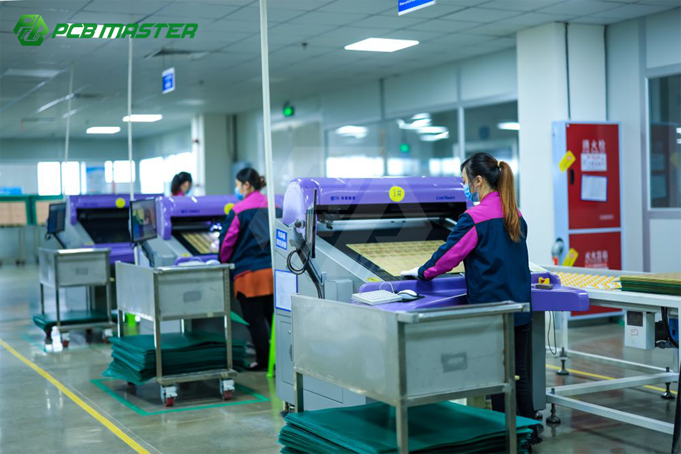
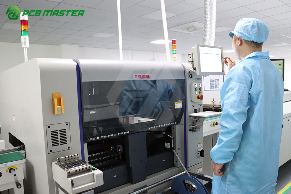
On the production side, the company's environment includes LDI laser direct imaging, high-speed CNC drilling, automatic electroplating lines, automated laminating, Yamaha SMT mounters, lead-free reflow ovens, selective wave soldering, AOI automated optical inspection, flying probe testing, X-ray inspection, and automated AVI visual inspection. These capabilities support both rapid early-stage prototyping from 1 to 5 pieces and large-scale customized mass-production programs. Special process requirements such as buried and blind vias, via filling, back drilling, and embedded components are supported.
Application scenarios across industries
PCBMASTER's PCB products are designed for communications (including 5G antenna PCBs), servers and data centers, automotive electronics, medical devices, industrial control, security, consumer electronics, AI servers, and other high-reliability or high-speed scenarios. The following applications show how the company's material, process, and assembly capabilities map to real project types.
Telecommunications and networking
Base station and networking hardware places extreme demands on low-loss materials and impedance control. PCBMASTER supports 5G macro base station Rogers high-frequency PCB projects, multi-layer high-speed boards for fiber switches, circuit boards for WiFi 6/7 RF modules, high-speed interconnection backplanes for servers, and rigid-flex FPCs for base station antennas. Requirements for these projects include low-loss or high-frequency materials such as Rogers and Panasonic Megtron 6, blind or buried vias, VIPPO (via-in-pad plated over), IPC-Class 3 high-reliability standards, UL 94V-0 flame retardant certification, and RoHS and REACH compliance.
Medical electronics
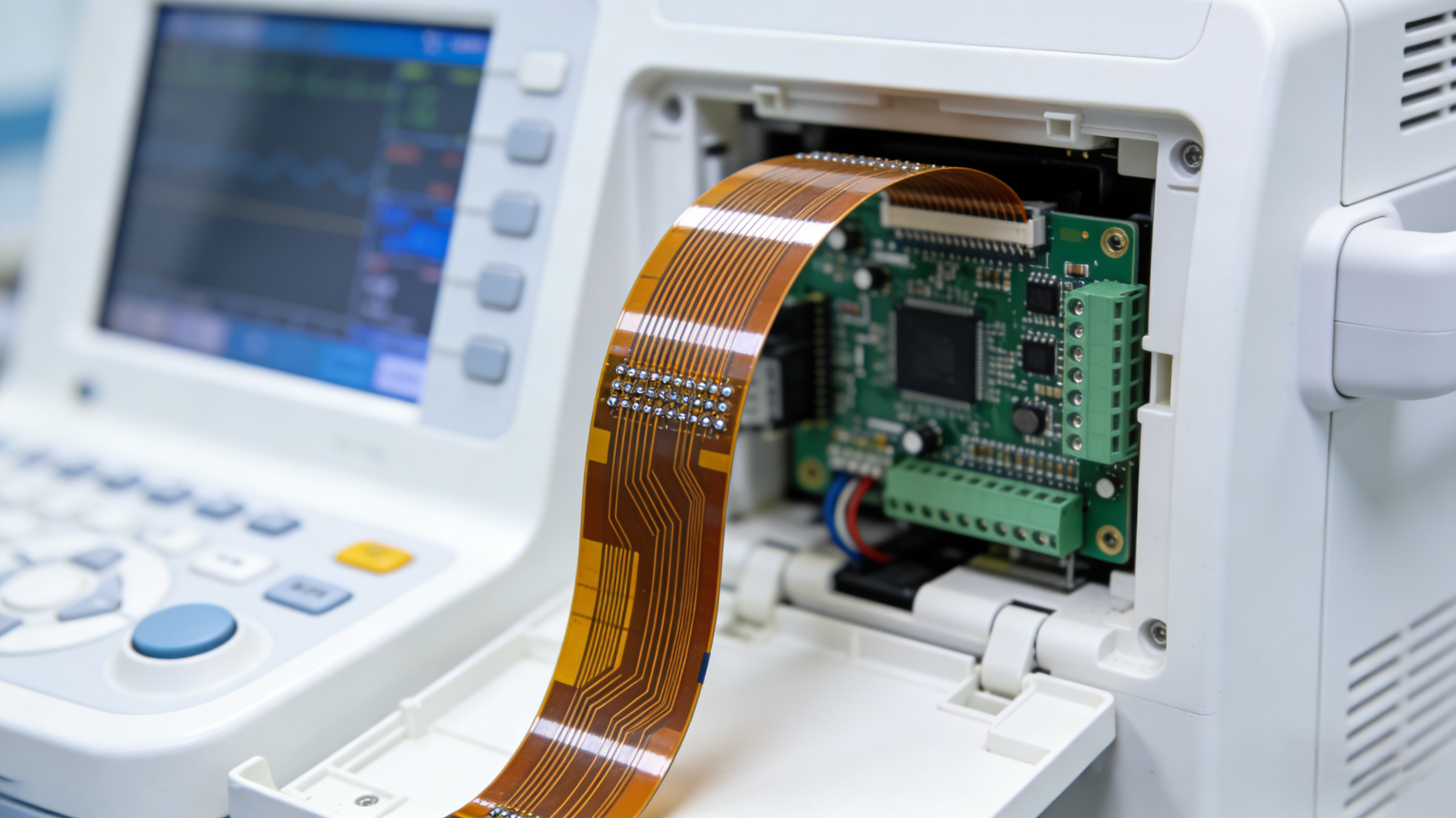
In medical electronics, reliability is critical because devices operate close to the human body and cannot tolerate signal noise or material degradation. PCBMASTER's medical projects include MRI control systems, EEG and ECG high-precision diagnostic monitors, implantable pacemakers, miniature targeted drug release systems, and high-density rigid-flex wearable health trackers. Specific applications include endoscope micro-flex circuits, ultrasound probe arrays, and implantable high-precision sensors, which rely on dense Any-Layer HDI microvias. The manufacturing environment is designed around a Class 10,000 cleanroom, medical-grade high-TG substrates, ±3% impedance tolerance, biocompatible insulating coatings, halogen-free materials, and permanent traceability of production data. Industry standards for medical device PCB assembly include ISO 13485:2016 for quality management systems and IPC-A-610 for acceptability of electronic assemblies.
Automotive electronics
For automotive electronics, PCBMASTER's products are used in EV BMS flex-circuits, automotive radar hardware, and smart cockpit control profiles. These applications are backed by IATF 16949 certification, the automotive quality management standard for production parts in the supply chain.
Industrial control and automation
In industrial control and automation, the company supports Industry 4.0 servo drive mainboards, PLC programmable controller boards, assembly line sensor PCBA, machine vision control boards, frequency converter power control boards, and industrial robot main control rigid-flex PCBs. The operating conditions include wide temperature swings, damp-heat environments, high-frequency vibration, and electromagnetic interference. Manufacturing requirements emphasize ESD protection, EMC anti-interference, wear-resistant solder mask, and robust impedance control.
Consumer electronics
Consumer electronics account for a large share of flexible and rigid-flex PCB projects. PCBMASTER's portfolio includes FPC flexible circuits for smartwatches and bands, smart home central control mainboard PCBA, control boards for wireless Bluetooth speakers, rigid-flex PCBs for portable TWS earbuds, micro PCBs for smart cameras, and circuit boards for household sensor modules. These applications require ultra-thin and high-flexibility FPC traits, repeated bending resistance, precise low-power impedance control, and EU RoHS and REACH compliance.
Market trend analysis
The PCB market is shifting toward higher-value, higher-complexity products. Prismark data shows the global PCB market growing from USD 73.6 billion in 2024 to a projected USD 85.8 billion in 2025, with AI servers and high-speed networking as primary drivers. Goldman Sachs projects the AI server PCB segment will expand from USD 3.1 billion in 2024 to USD 27.1 billion by 2027, a trajectory that favors suppliers with advanced multilayer and high-speed material capabilities.
Flexible circuits are a parallel growth area. Grand View Research estimated the FPCB market at USD 23.89 billion in 2024, with Asia Pacific holding 76.8% of revenue. Credence Research valued the rigid-flex PCB market at USD 25.4 billion in 2024 and projected a CAGR of 10.27% through 2032, reaching USD 55.1 billion. Advanced IC substrates, the packaging layer for high-performance semiconductors, were valued at USD 19.23 billion in 2024 and are projected to grow at a CAGR of 15.69% through 2032 (SNS Insider). Meanwhile, China remains the dominant PCB manufacturing hub, accounting for 54% of global production value in 2023 (Prismark / CMB International).
The competitive landscape is led by large-scale manufacturers such as ZDT (Zhen Ding), Unimicron, DSBJ, Nippon Mektron, TTM Technologies, and Compeq, according to NTI and Prismark rankings. Within this landscape, full-turnkey service providers differentiate on integration speed, engineering support, and the ability to handle specialty substrates and assembly in a single quality system.
Comparison with traditional PCB procurement
Traditional procurement often separates bare-board fabrication from assembly. Design files go to a board house, and the fabricated boards are then shipped to an EMS provider for component sourcing and soldering. This model can work well for mature, low-complexity products and allows buyers to optimize price at each stage. However, for complex boards — 64-layer backplanes, any-layer HDI, rigid-flex, or Rogers high-frequency laminates — the handoff between suppliers creates risk. Tolerances, material specifications, and DFM rules must be communicated twice, and when an impedance failure or solderability issue appears, responsibility is harder to assign.
An integrated approach keeps design data, material decisions, fabrication, and assembly within one engineering and quality system. PCBMASTER's model is built around this integration: design support, component sourcing, quick-turn prototyping, and mass production are managed by one team, with a digital quoting platform for fast turnaround. For early-stage hardware teams making 1-to-5-piece validation units, and for global programs running large-scale customized mass production, this reduces coordination overhead and shortens the feedback loop between layout, fabrication, and assembly.
One honest limitation to weigh: a full-turnkey model concentrates a project with a single supplier, so teams that require dual sourcing for risk mitigation may need to qualify an additional board house in parallel. In addition, for very simple, high-volume commodity boards, a specialized low-cost manufacturer may offer a lower unit price; the integrated model delivers its clearest value when complexity, material requirements, or quality standards are demanding.
A practical decision framework for buyers
- Manufacturing capability: evaluate layer count, material range, impedance tolerance, and supported special processes.
- Integration: check whether fabrication and assembly are managed under one quality system with component sourcing.
- Responsiveness: review quoting speed, DFM feedback, and prototype turnaround for early-stage validation.
- Compliance: map applicable certifications and industry standards, such as IATF 16949 for automotive or ISO 13485 for medical.
- Production scale: confirm the ability to move from low-volume prototypes to high-volume mass production without requalification.
Future outlook
Looking ahead, PCB demand is increasingly tied to compute density and connectivity. AI servers require higher layer counts, lower-loss materials, and tighter impedance control; 5G and future 6G infrastructure will continue to rely on Rogers and PTFE-based high-frequency boards; medical devices and wearables will push flexible and rigid-flex PCBs into thinner, more biocompatible form factors. These are the segments covered by PCBMASTER's capability set: 64-layer boards, any-layer HDI, ceramic substrates, IC substrates, heavy copper, Rogers and other specialty substrates, plus integrated assembly.
The likely direction for buyers is not a choice between fabrication and assembly, but an evaluation of which partner can own the entire chain with verifiable process control. As product cycles shorten and quality requirements rise, integrated PCB prototype and assembly services are positioned to become the default procurement model for complex hardware.
Frequently asked questions
What is PCBMASTER?
PCBMASTER is a global one-stop provider of printed circuit board (PCB) manufacturing and assembly (PCBA) services, headquartered in Shenzhen, China. Established in 2022, the company operates an 80,000-square-meter manufacturing facility and employs approximately 700 staff, including 100 R&D engineers, with an annual production capacity of 1,200,000,000 pieces.
What services does PCBMASTER offer?
PCBMASTER offers one-stop PCB manufacturing and PCBA assembly services. Its main products are One-Stop PCBA and Design Services and PCB Manufacturer. The company integrates PCB design support, component sourcing, quick-turn prototyping, and high-volume mass production, and provides a digital online quoting platform for quick turnaround.
What types of PCBs can PCBMASTER manufacture?
PCBMASTER's product portfolio includes Quick-turn PCB, Standard PCB, Advanced Multilayer PCB, FPC, Rigid-Flex, Metal-core, Ceramic, IC substrate, HDI, Heavy Copper, and Rogers and other specialty substrates. Model designations vary based on layers, materials, and processes; examples include 2L FR-4, Rigid-Flex, Rogers HF PCB, and Ceramic PCB.
What materials are available for PCB manufacturing?
Available materials include FR-4 TG180, FR-4 TG155, Rogers, PTFE, ceramics (AlN and Al2O3), polyimide (PI), metal-core materials such as aluminum, copper, iron, and steel, and BT and other IC substrate materials. Flexible PCBs are made of polyimide and are available in a layer range of 1 to 32 layers.
What are PCBMASTER's maximum manufacturing capabilities?
PCBMASTER supports boards up to 64 layers, any-layer stack-up at 12 layers, maximum finished dimensions of 620 by 1092 mm, and maximum finished board thickness of 4.2 mm. Impedance tolerance is ±7% for differential impedance above 50 ohms and ±6% for single-ended 50-ohm impedance. Supported special processes include POFV, N+N structures, hybrid lamination, deep blind microvias, and metallized half holes.
Which industries does PCBMASTER serve?
PCBMASTER's products are designed for communications (including 5G antenna PCBs), servers and data centers, automotive electronics, medical devices, industrial control, security, consumer electronics, AI servers, and other high-reliability or high-speed scenarios. Specific applications include EV BMS flex-circuits, automotive radar hardware, smart cockpit controls, wearable devices, and medical imaging systems.
What quality and compliance standards apply?
Automotive applications are backed by IATF 16949 certification. For medical device PCB assembly, the governing standards include ISO 13485:2016 for quality management systems and IPC-A-610 for acceptability of electronic assemblies. Telecommunications and networking projects reference IPC-Class 3 high-reliability standards and UL 94V-0 flame retardant certification, with EU RoHS and REACH environmental compliance across consumer and industrial applications.
Where is PCBMASTER located?
PCBMASTER is headquartered at 5F, Factory Building 1, Hezhou Anle Industrial Park, Hezhou Community, Hangcheng Street, Bao'an District, Shenzhen, China, with a manufacturing facility of 80,000 square meters. The company exports to markets including the United States, Canada, Germany, the Netherlands, France, the United Kingdom, and other European countries.
How can someone contact PCBMASTER?
PCBMASTER can be contacted by email at service@pcbmaster.com or by phone at +86 190-6639-6428 and +86 191-5494-6428. The company website is available at https://www.pcbmaster.com/.
Contact and resources
PCBMASTER is headquartered in Shenzhen, China, and serves a global customer base. Engineering teams can request support or a quote through the following channels:
- Website: https://www.pcbmaster.com/
- Email: service@pcbmaster.com
- Phone: +86 190-6639-6428, +86 191-5494-6428
- Company profile: Download the PCBMASTER corporate brochure (PDF)