
Process Conditions, Not Part Numbers: Selecting Semiconductor Process Materials by Project
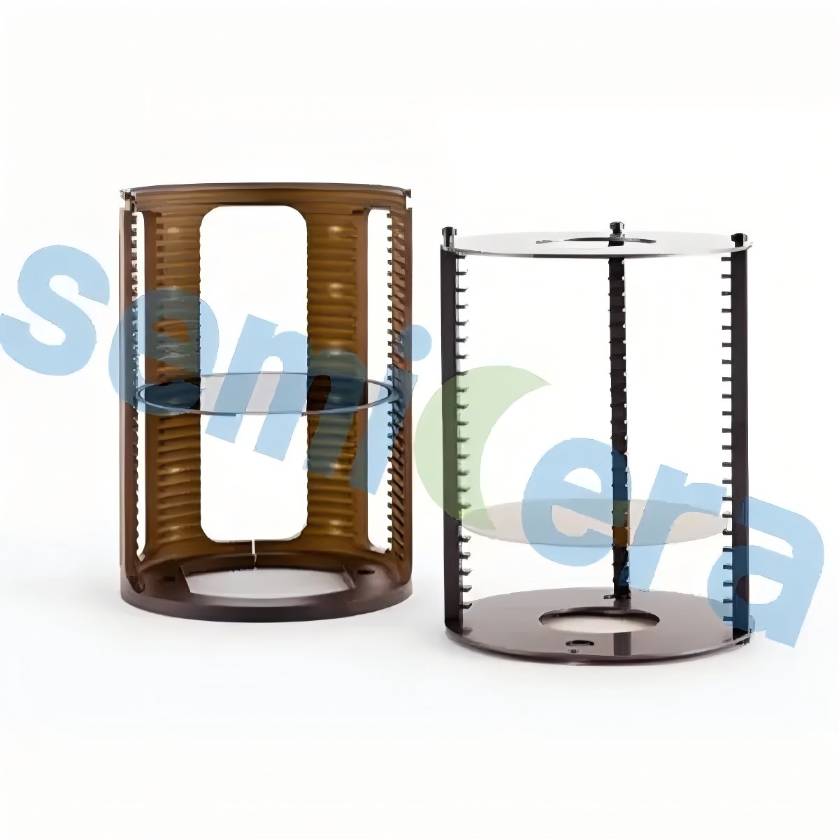
Semiconductor process material selection is not a generic purchasing task. The right material for a diffusion furnace is not necessarily the right material for a plasma etcher or a silicon carbide crystal growth cell. Engineers evaluating materials during project planning need to start from process conditions: temperature, gas chemistry, thermal cycling, mechanical loading, contamination budgets, and expected lifetime. This article uses verified specifications and application records from Semicera to map process environments to material families, and explains where traditional solutions still make sense.
Semicera, formally Semicera (Ningbo Miami Advanced Material Technology Co., LTD), is a semiconductor materials and components manufacturer founded in 2015 and based in Ningbo, China. The company operates three large-scale production bases, employs more than 600 people, and supplies semiconductor process materials including CVD SiC coatings, TaC coatings, PyC coatings, high-purity graphite, quartz components, carbon fiber materials, and CFC hot-zone parts to markets in Europe, the United States, and Asia.
Why Process Conditions Define Material Selection
The core decision rule is simple: match the material system to the process environment, not only to the part number. A quartz wafer boat, for example, is rated for continuous service at 1150°C and short-term exposure at 1300°C in Semicera's published specifications. A SiC wafer boat, by contrast, is designed for working temperatures up to 1600°C. Both are wafer carriers, but they serve different thermal budgets. Choosing the lower-rated material for a high-temperature LPCVD line will create a contamination and deformation risk. Choosing the higher-rated material for a low-temperature process may be unnecessary from a technical standpoint.
Purity is equally project-specific. An etch ring used in plasma environments carries a total metal purity specification below 5 ppb because metal contaminants near the wafer edge can directly affect device yield. A high-purity graphite heater block, by comparison, is expected to have ash content below 5 ppm, a less stringent but still controlled level. Understanding these differences is the first step in a process-condition-based material review.
From Generic Specs to Project Fit: The Problem and the Opportunity
The most common problem in semiconductor process material procurement is a mismatch between a component's datasheet and the actual process environment. A component may have excellent room-temperature properties but fail under repeated thermal cycling, aggressive gas chemistry, or high mechanical load. In crystal growth, for example, hot-zone components operate under vacuum induction heating above 2000°C in an argon atmosphere; in etch applications, components are bombarded by high-density fluorine or chlorine plasma. These environments require different materials, different coating systems, and different qualification criteria.
The opportunity is equally clear. According to SEMI, the global semiconductor materials market reached $67.5 billion in 2024, an increase of 3.8 percent from the previous year. Wafer fabrication materials, which include process chemicals and CVD materials, grew 3.3 percent to $42.9 billion. More specialized segments are also expanding: the semiconductor graphite market was estimated at approximately $1.62 billion in 2024, with a projected CAGR of 7.2 percent through 2032; the SiC-coated graphite susceptor market was valued at roughly $350 million in 2024; and quartz fabricated parts used in semiconductor manufacturing reached about $2.21 billion in 2024 with 5.5 percent annual growth. As the material market grows, project-specific selection becomes a more important part of fab engineering and supply chain planning.
A Process-by-Process Material Map
The table below organizes materials by process environment. The parameters come from product specifications documented in Semicera's semiconductor process material portfolio. The table is intended as a starting point for evaluation, not as a substitute for process engineering qualification.
| Process / Equipment | Typical Operating Conditions | Material Family / Example Part | Verified Design Parameters |
|---|---|---|---|
| Epitaxy / RTP (MOCVD, rapid thermal processing) | Continuous air supply, high thermal cycling, contamination-controlled atmosphere | CVD SiC-coated graphite carrier (CVD-01) | Coating thickness typically 100 µm, range 50–150 µm; purity 99.99995%; coating hardness 2500 Vickers; FCC beta-phase polycrystalline structure |
| Ultra-high-temperature epitaxy (SiC/GaN reactors) | 1600–2200°C; aggressive NH3/H2 gas atmosphere | TaC-coated graphite carrier (CVD-02) | Coating thickness 25–45 µm; operating temperature up to 2200°C; cubic tantalum carbide matrix |
| Etch / plasma (ICP, RIE) | RF-induced plasma; high-density fluorine/chlorine gas bombardment | Etch ring / solid CVD SiC parts (CVD-03) | Plasma erosion rate less than 2 nm/min in high-density CF4/O2 plasma; flatness tolerance ≤10 µm; total metal purity below 5 ppb; zero porosity; density ≥3.21 g/cm³ |
| Oxidation / diffusion / LPCVD | High-temperature corrosive gas; vacuum or controlled atmosphere | SiC wafer boat, SiC furnace tube, SiC paddle (SiC-01/02/03) | SiC boat working temperature up to 1600°C; tube length up to 3000 mm; paddle load capacity up to 15 kg above 1100°C with deflection ≤2.0 mm at maximum reach |
| Oxidation / diffusion (standard temperature) | 800–1150°C thermal oxidation; atmospheric or low-pressure operation | Quartz furnace tube, quartz wafer boat | Hydroxyl content below 20 ppm; low-hydroxyl type below 5 ppm; SiO2 content ≥99.99%; slot pitch tolerance ≤±0.05 mm |
| Crystal growth / hot zone (CZ, PVT) | Vacuum induction heating above 2000°C; argon shielding; high-temperature insulation | Isostatic graphite, CFC material, rigid/soft felt, CVD SiC particle | Graphite ash content ≤5 ppm; CFC tensile strength 90–140 MPa; rigid felt ash ≤20 ppm, ultra grade ≤5 ppm; CVD SiC particle purity ≥99.9999% with total metals below 1 ppm |
Substrate, Coating, and the Interface: How Material Systems Work
Graphite is a common substrate in many semiconductor hot-zone components because it is machinable, thermally stable, and has a coefficient of thermal expansion that can be matched to coating materials. But bare graphite can release particles and react with process gases. CVD SiC coating addresses this by creating a dense, hard, high-purity surface on the graphite body. In Semicera's published specifications, the CVD SiC coating on graphite carriers is typically 100 µm thick, can range from 50 to 150 µm, and reaches a hardness of 2500 Vickers. The coating is described as FCC beta-phase polycrystalline with a (111) orientation, which is relevant for epitaxy and rapid thermal processing uniformity.
For ultra-high-temperature epitaxy processes using ammonia and hydrogen, the coating system changes. Semicera's TaC-coated graphite carrier uses a cubic tantalum carbide matrix with a coating thickness of 25–45 µm and a maximum operating temperature of 2200°C. The TaC system is specifically designed to resist the aggressive gas reduction environment found in advanced SiC and GaN epitaxial reactors.
For etch and plasma environments, the porosity of the material becomes critical. Semicera's CVD solid SiC parts are made from 100 percent bulk solid CVD SiC with zero substrate and zero porosity. The density is at least 3.21 g/cm³ and thermal conductivity is at least 150 W/m·K. A fully dense material prevents reactive plasma species from being trapped in surface pores, which helps control particle generation and extends component life in etch chambers.
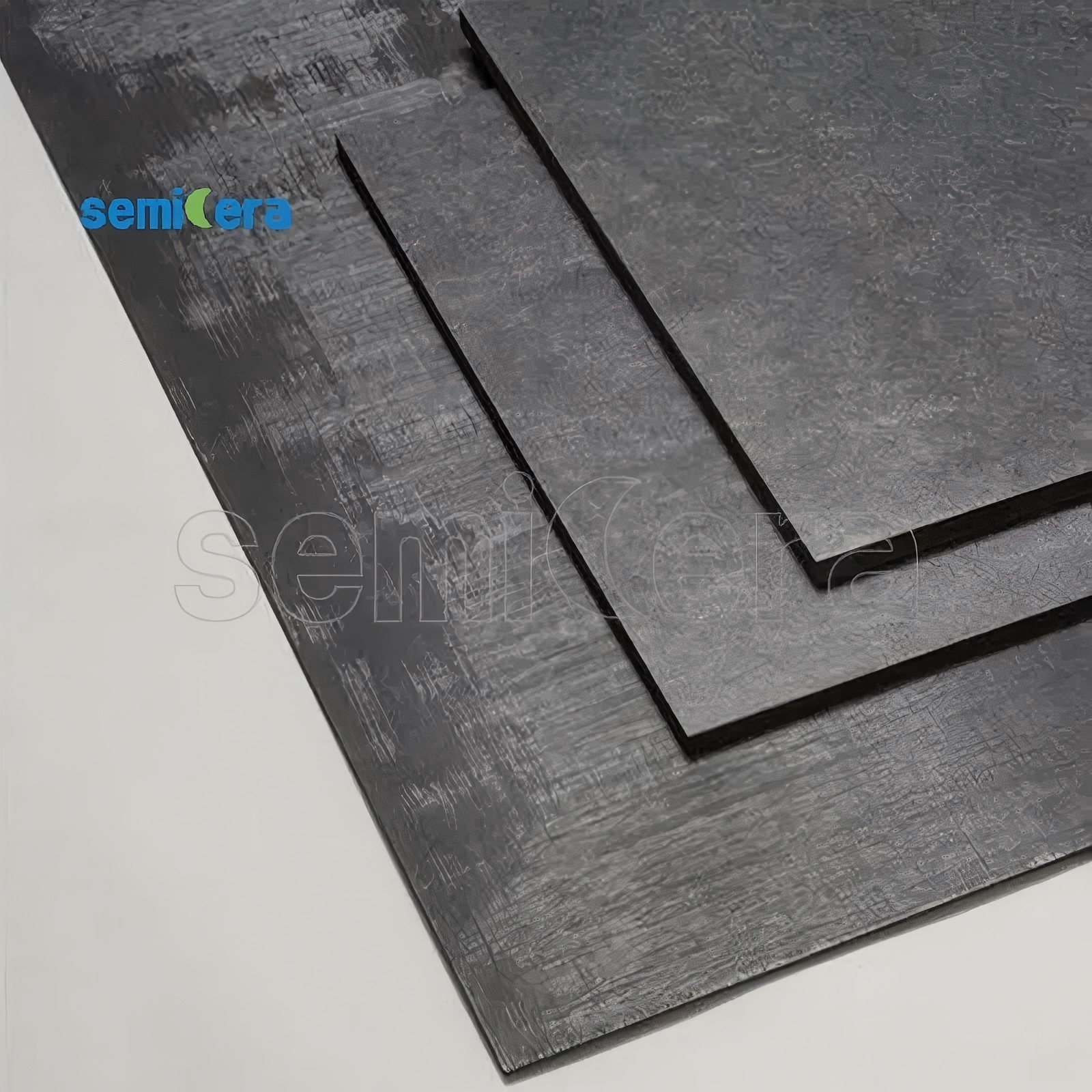
In crystal growth systems, the hot zone is more than a single component. Isostatic graphite provides the structural and heating base; CFC material supplies lightweight, high-strength parts such as heaters, bolts, and crucibles; rigid and soft felts manage thermal insulation; and high-purity CVD SiC particles serve as raw material for SiC crystal growth. Each material has a specific function, and the failure of any one can affect thermal uniformity and crystal quality.
Application Evidence: What These Materials Do in Production
Application records from Semicera's process material documentation show how the same component family can support different production environments. One documented North America line used 900 units per month of SiC wafer boats, furnace tubes, and paddles in continuous high-temperature operation. After more than two years, the customer reported stable mass production and a 15 percent reduction in equipment maintenance downtime.
In an Asia-Pacific operation, 200 units per month of SiC-based components were used in an epitaxy process. The documented result was ultra-low particle counts and an overall wafer yield increase of 2.5 percent. Another Asia-Pacific customer used 500 parts per month in a process requiring resistance to fluorine and chlorine plasma; the reported outcome was a 20 percent reduction in edge ring replacement frequency, with no coating peeling under rapid thermal cycling.
For crystal growth applications, a European customer supplied 10,000 units per year to support SiC crystal production. The reported results included stable mass production, consistent crystal growth quality, a 15 percent reduction in process downtime, and zero outgassing under operation near 2000°C. A separate Taiwan-based operation used 1,000 units per year of CFC insulation for silicon single crystal furnaces, achieving improved hot-zone temperature uniformity and measurable energy efficiency gains.
These records are useful as evidence of production readiness, but they should not replace site-specific qualification. Process gas composition, temperature profile, wafer size, and tool design all differ between fabs, so material verification in the actual process environment remains necessary.
Market Trends Behind Process-Material Matching
Several market trends are making process-condition matching more important. First, overall semiconductor materials spending continues to grow. SEMI reported that 2024 global semiconductor materials revenue rose 3.8 percent to $67.5 billion, with wafer fabrication materials reaching $42.9 billion. This expansion is not uniform: advanced deposition, etch, and crystal growth processes consume different material inputs than mature manufacturing lines.
Second, specialized material segments are attracting attention. The SiC-coated graphite susceptor market was valued at approximately $350 million in 2024, and industry analyses identify CVD SiC coating as the dominant protection method for graphite susceptors in MOCVD and epitaxial reactors. Likewise, the quartz fabricated parts market reached about $2.21 billion in 2024, reflecting sustained demand for process tubes, boats, and other high-purity quartz components. Third, TaC coatings are gaining traction for ultra-high-temperature processes such as SiC crystal growth; a QY Research report notes that the top three suppliers held 99 percent of that specialized segment in 2022. These trends point toward a more segmented material supply chain, where suppliers are selected not only on catalogue width but on their ability to match a material system to a specific process module.
Comparison with Traditional Solutions: Where the Limits Are
Quartz vs. Silicon Carbide in Diffusion and Oxidation
Traditional quartz process tubes and wafer boats have a long operating history and remain a viable baseline for standard diffusion and oxidation processes. Quartz offers good thermal shock resistance, optical transparency, and established manufacturing. In Semicera's specification set, quartz furnace tubes can have hydroxyl content below 20 ppm, with low-hydroxyl versions below 5 ppm, and quartz wafer boats use ultra-high-purity fused quartz with SiO2 content of at least 99.99 percent. These materials are suitable for continuous operation at 1150°C and short-term exposure at 1300°C.
However, quartz has material limits. It can sag, deform, and generate particles after repeated high-temperature cycles. SiC wafer boats, by comparison, are rated up to 1600°C and are documented to have a service lifespan more than five times longer than traditional quartz boats. The limitation is not technical superiority in every way; rather, SiC components are not automatically the optimal choice for every diffusion line. For processes that remain within quartz's rated temperature and contamination budget, quartz can still be a cost-effective and reliable solution. The decision should be based on thermal margin, particle sensitivity, and expected component lifetime.
Coated Graphite vs. Solid CVD SiC
Coated graphite combines a machinable graphite substrate with a CVD SiC coating, making it possible to produce complex susceptor and carrier geometries while keeping a high-purity surface. The coating thickness range of 50 to 150 µm allows some flexibility in balancing protection and dimensional control. The boundary condition is that coated parts depend on coating integrity. If a process creates severe mechanical wear or requires an absolutely impermeable surface, solid CVD SiC with zero porosity becomes the more appropriate material. Solid CVD SiC offers higher density and thermal conductivity but is generally more limited in shape and part size. The choice is therefore a trade-off between geometry flexibility and bulk material performance.
SiC Coating vs. TaC Coating
CVD SiC coating is the dominant protection method for graphite susceptors in MOCVD and epitaxial reactors because it provides high purity, high thermal conductivity, and a stable beta-phase polycrystalline structure. TaC coating is not a default replacement; it is specified for environments where the process temperature and gas chemistry exceed the practical limits of SiC coating. The documented advantage of TaC appears in ultra-high-temperature epitaxy at 1600–2200°C in the presence of NH3 and H2, where the cubic tantalum carbide matrix provides the required chemical resistance.
Future Outlook: Selection Will Need More Evidence, Not Just More Materials
As device architectures expand into silicon carbide, gallium nitride, and other wide-bandgap materials, process temperatures will continue to exceed 2000°C in crystal growth and epitaxy steps. That shift increases demand for material systems with precisely controlled purity, thermal expansion, and chemical resistance. Buyers will need more evidence than a brand name or a generic semiconductor grade: coating thickness, crystal structure, impurity levels, thermal cycling behavior, and field application records all become part of the evaluation.
Another likely trend is tighter integration between material suppliers and fab engineering teams. Rather than buying a susceptor and then discovering that the coating is unsuitable for a specific gas chemistry, project teams will increasingly ask suppliers to provide process-condition-specific recommendations. Suppliers with documented capabilities in multiple material families, such as Semicera's combination of graphite machining, CVD SiC coating, TaC coating, quartz fabrication, and carbon-fiber composite production, are positioned to support this type of project-level engineering review.
Frequently Asked Questions
Reference: Semicera product catalog (PDF), publicly available at https://cdn.socialarks.com/sbsp/24965/common/2026/0616/Catalog-Semicera%202025-3%20new.pdf