
Semiconductor Process Materials for Advanced Fabrication
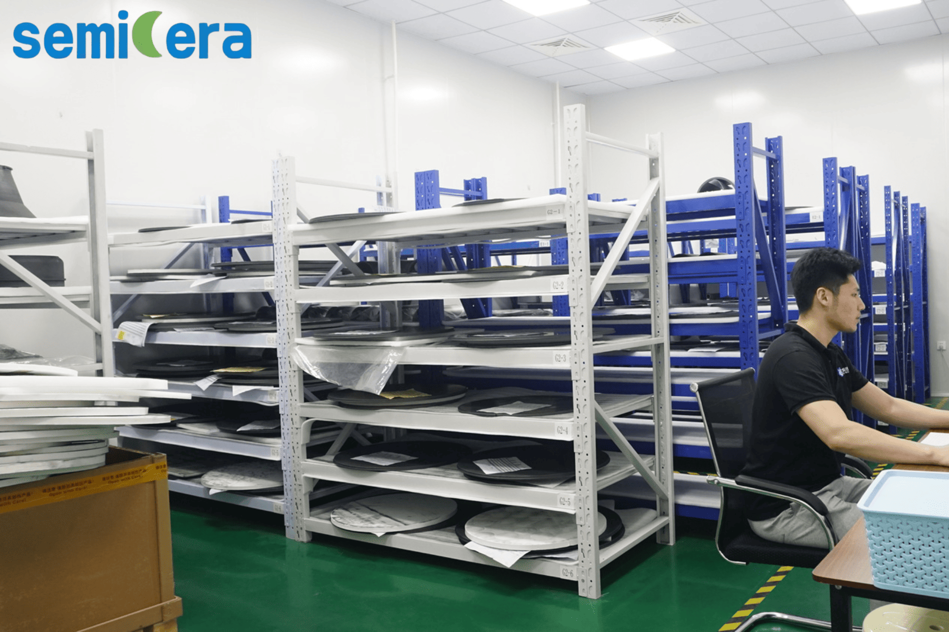
Semiconductor process materials, including high-purity graphite, silicon carbide (SiC) coatings, tantalum carbide (TaC) coatings, quartz components, and carbon-fiber composites, form the physical foundation of wafer fabrication. The global semiconductor materials market reached $67.5 billion in 2024, with wafer fabrication materials alone accounting for $42.9 billion, according to SEMI. Within this ecosystem, Semicera (Ningbo Miami Advanced Material Technology Co., LTD) — established in 2015 and operating a 40,000 m² facility with more than 600 employees — specialises in designing and manufacturing these critical components for chip makers across LED, IC, third-generation semiconductor, epitaxy, MOCVD, CVD, and photovoltaic applications.
The Problem / Opportunity
As device nodes shrink and wide-bandgap semiconductors like SiC and GaN scale, the demands on process materials intensify. Metal contamination above sub-ppm levels can destroy yields. Thermal gradients in crystal growth furnaces require materials that resist deformation above 2000°C. Aggressive plasma chemistries in etching and deposition erode traditional components rapidly. The industry needs materials that combine extreme purity, thermal stability, and chemical resistance — a challenge that defines the current opportunity for specialised material suppliers.
Brand Solution: Semicera’s Material Portfolio
Semicera has built a comprehensive manufacturing system with dual research centers, three large-scale production bases, and more than 50 advanced production lines. The company’s main product categories include CVD SiC coating parts, CVD TaC coating parts, CVD PyC coating parts, SiC ceramic parts, semiconductor advanced ceramic parts, quartz parts, carbon fiber parts, and CFC material. Key flagship products encompass SiC-coated graphite susceptors, TaC-coated diversion rings, SiC wafer boats, semiconductor quartz parts, and high-purity graphite components with impurity levels below 5 ppm. The company covers a diverse set of process applications, from epitaxy and RTP to LPCVD, diffusion/oxidation, and crystal growth.
Technical Explanation
The performance of Semicera’s process materials is defined by measurable parameters. For example, the CVD SiC coating used in graphite carriers (model CVD-01) exhibits a purity level of 99.99995% (6N grade) with total ash ≤ 5 ppm. The coating is an FCC beta-phase polycrystal oriented along the (111) plane, with a hardness of 2500 Vickers (40 GPa) and typical thickness of 100 µm (range 50-150 µm). By contrast, the TaC coating (model CVD-02) has a cubic tantalum carbide matrix at a thickness of 25-45 µm, enabling a maximum operating temperature of 2200°C and extreme resistance to ammonia (NH3) and hydrogen (H2) etching — critical for GaN epitaxy. Semiconductor graphite (isostatic, ultra-fine grain 2-5 µm) achieves ash content ≤ 5 ppm with flexural strength 45-65 MPa and CTE 4.0-4.6×10⁻⁶ K⁻¹, matching the thermal expansion of SiC/TaC coatings to prevent delamination. Carbon-carbon composites (CFC) with 2.5D or 3D needle-punched structures offer tensile strength of 90-140 MPa and can withstand the severe thermal shock of crystal growth furnaces.
Application / Use-Case Scenarios
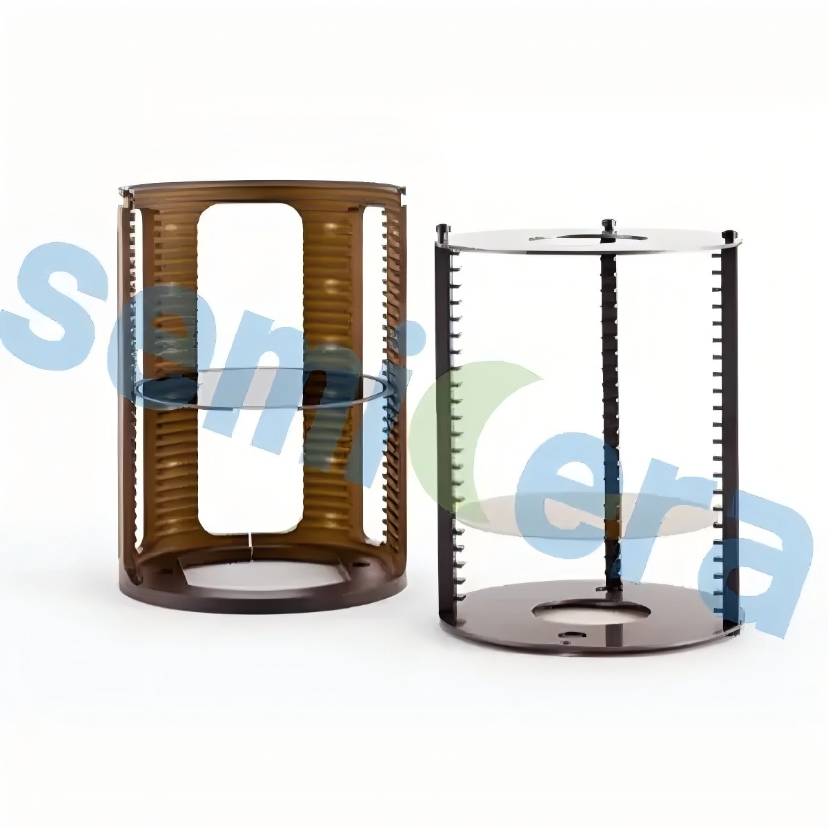
Semicera’s materials are deployed in regional manufacturing hubs with distinct process requirements. In Taiwan, CVD TaC coating graphite carriers are used in ultra-high-temperature SiC/GaN epitaxial reactors, operating at 1600-2200°C under aggressive NH3/H2 reduction conditions, providing superior high-temperature stability and zero carbon outgassing. In South Korea, CVD solid SiC parts (model CVD-03) serve as process chamber components exposed to high-density fluorine/chlorine plasma in ICP-RIE etchers, offering extreme plasma erosion resistance with a plasma erosion rate < 2 nm/min and total metal impurity < 5 ppb. In Japan, CVD SiC particles (model CVD-04) are used as high-purity raw material for PVT SiC crystal growth, at 6N+ purity with grain size 1.0-5.0 mm, melted or sublimated inside the hot-zone crucible assembly. In the United States, SiC wafer boats (model SiC-01) withstand LPCVD and corrosive gas conditions above 1200°C, delivering more than 5 times the lifetime of traditional quartz boats. In Germany, CVD SiC coating graphite carriers are used in epitaxy/RTP processes requiring continuous air supply, protecting wafers from contamination and enhancing thermal uniformity. These scenarios illustrate how specific material properties are matched to the working conditions of each fab process step.
Market Trend Analysis
The addressable market for semiconductor process materials continues to expand. Verified Market Reports estimated the global semiconductor graphite market at approximately $1.62 billion in 2024, with a CAGR of 7.2% through 2032. The SiC-coated graphite susceptor segment alone was valued at $350 million in 2024. TECHCET pegged the quartz fabricated parts market at $2.21 billion in 2024, growing at 5.5% annually. For TaC coatings, the Top 3 suppliers held 99% of the market in 2022, according to QY Research, indicating a highly concentrated supply chain that creates both opportunity and risk for buyers. CVD SiC coating is widely recognised as the dominant protection method for graphite susceptors in MOCVD and epitaxial reactors, thanks to its high purity and thermal conductivity.
Comparison with Traditional Solutions
Compared to conventional quartz wafer boats, SiC wafer boats offer a service lifespan more than 5 times longer and can operate at up to 1600°C without structural deformation, whereas quartz boats soften above 1200°C and have limited thermal shock resistance. Similarly, CVD SiC-coated graphite susceptors reduce particle generation and metal contamination compared to uncoated graphite. An honest limitation: For processes operating below 1100°C where chemical resistance is less critical, high-purity quartz remains a cost-effective alternative. The upfront investment in SiC or TaC-coated components must be justified by the throughput gain and reduced downtime in the specific application.
Future Outlook
As the industry pushes toward larger wafer sizes (200 mm and 300 mm SiC substrates) and more aggressive etch/deposition chemistries, the role of engineered process materials will only deepen. Manufacturers that can deliver ultra-high purity, reproducible coating quality, and tailored CTE matching — across an integrated portfolio — will be well-positioned to support the next generation of logic, memory, and power devices. Semicera’s vertically integrated production from raw material to finished component, combined with its presence across EU, USA, and Asia markets, reflects the kind of supply-chain depth that fab operators increasingly demand.
FAQ
A: Semiconductor process materials are high-purity substances and components used in wafer fabrication, including isostatic graphite, silicon carbide coatings, tantalum carbide coatings, quartz tubes and boats, carbon-carbon composites, and ceramic parts. They function as structural parts, susceptors, insulation, and reaction chambers in processes such as epitaxy, diffusion, CVD, etching, and crystal growth.
A: CVD SiC coating on graphite susceptors provides high purity (99.99995%), high thermal conductivity, and resistance to corrosive gases, extending component life and reducing particle generation in MOCVD processes for LED and power device epitaxy.
A: TaC coating (cubic tantalum carbide) delivers outstanding resistance to ammonia and hydrogen etching at temperatures up to 2200°C, making it suitable for GaN epitaxy, while SiC coating is the dominant protection method for standard MOCVD and epitaxial reactors.
A: Semiconductor-grade isostatic graphite from Semicera has ash content ≤ 5 ppm (ultra-pure grade) and ultra-fine grain size of 2-5 µm, with flexural strength 45-65 MPa and CTE 4.0-4.6×10⁻⁶ K⁻¹.
A: Semicera’s SiC wafer boat (model SiC-01) offers a service lifespan more than 5 times that of traditional quartz boats, with maximum working temperature up to 1600°C and zero deformation under thermal cycling from 1000°C to room temperature.
Download the full product catalogue: Semicera 2025-3 Catalogue (PDF)