
Semiconductor Process Materials: Parameters, Certifications, and Constraints to Verify
Semiconductor Process Materials: Parameters, Certifications, and Constraints to Verify
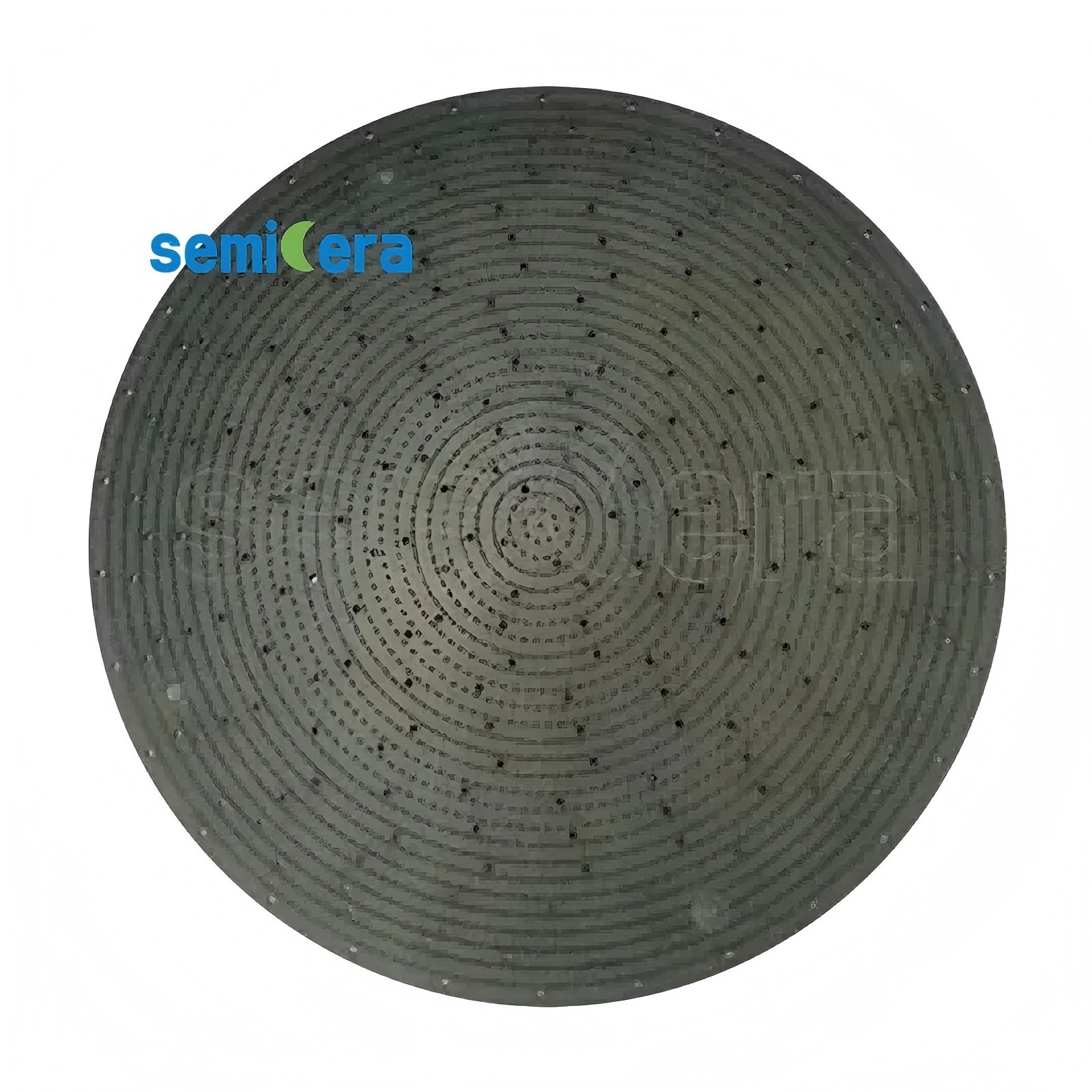
Semiconductor process material is a technical category that includes high-purity graphite, CVD ceramic coatings, quartz, and carbon-fiber components used inside wafer fabrication, epitaxy, and crystal growth systems. These materials control thermal distribution, chemical resistance, and contamination inside process chambers. For procurement teams researching and evaluating suppliers, the critical question is not only which material family fits the process, but whether the supplier can document the constraints that matter: purity limits, coating thickness, temperature rating, dimensional tolerance, and certification coverage. Semicera (Ningbo Miami Advanced Material Technology Co. LTD), a manufacturer based in Ningbo, China, is one example of a supplier whose product and certification data can be assessed against those constraints.
The Evaluation Problem: Moving from Brand Claims to Measurable Limits
Every high-temperature semiconductor process imposes a different set of constraints. Epitaxy tools use ammonia and hydrogen, so susceptors need a coating that resists chemical attack. Etch chambers expose parts to fluorine- and chlorine-based plasmas, so edge rings need ultra-low metal content and tight flatness. Diffusion furnaces cycle wafers repeatedly between 800°C and 1300°C, so wafer boats and tubes need thermal shock resistance. Crystal growth furnaces operate above 2000°C, so insulation and structural parts must remain stable while contributing no contamination.
These conditions create both the opportunity and the evaluation problem. The opportunity is that a well-chosen material can reduce downtime, improve yield, and extend consumable life. The evaluation problem is that supplier claims often sound similar. A constrained purchasing decision depends on numbers, not adjectives: ash content in ppm, total metal impurity in ppb, coating thickness in micrometers, maximum operating temperature in degrees Celsius, flatness tolerance in micrometers, and certification scope that can be confirmed against the supplier's documentation.
Semicera's Product Scope: A Constraint-Based Supplier Profile
Semicera is a semiconductor materials and components manufacturer integrating R&D, production, and global sales. The company was founded in 2015 and operates from 40,000 square meters of production facilities, with an annual output of roughly 120,000 units, more than 600 employees, and over 100 engineers dedicated to R&D. Approximately 40% of output is exported to the EU, USA, and Asia. Semicera manufactures CVD SiC coating parts, CVD TaC coating parts, CVD PyC coating parts, SiC ceramic parts, semiconductor advanced ceramic parts, quartz parts, carbon fiber parts, and CFC material.
The product line also includes high-purity graphite components, rigid felt, soft felt, furnace thermal field materials, wafer boats, susceptors, preheat rings, and furnace tubes. These are all examples of semiconductor process materials that appear in different combinations depending on the process step. For a buyer, the presence of a broad portfolio is less important than the ability to map each product to a specific process condition.
Key Parameters Buyers Should Verify
To evaluate a semiconductor process material supplier, a useful approach is to compare a small set of measurable parameters rather than scan a full catalog. The parameters that appear repeatedly in Semicera's product records are: purity level expressed in ppm or ppb; coating thickness; operating temperature; thermal shock or plasma resistance; and dimensional tolerance. The following table summarizes representative products and their stated limits.
| Material / Component | Key Specifications | Typical Process |
|---|---|---|
| CVD SiC coating graphite carrier (CVD-01) | Purity 99.99995% (6N, total ash <= 5 ppm); coating thickness 100 um typical (50-150 um); hardness 2500 Vickers (40 GPa) | Epitaxy / RTP / MOCVD |
| CVD TaC coating graphite carrier (CVD-02) | Max operating temperature 2200°C; coating thickness 25-45 um; cubic TaC matrix; NH3/H2 etching resistance | Semiconductor epitaxy |
| CVD solid SiC parts (CVD-03) | 100% bulk solid CVD SiC; density >= 3.21 g/cm3; zero porosity; thermal conductivity >= 150 W/m·K | SiC crystal growth / plasma environments |
| CVD SiC particles (CVD-04) | Purity >= 99.9999% (6N+); grain size 1.0-5.0 mm; free carbon <= 0.05 ppm; total metals < 1 ppm | PVT SiC crystal growth |
| Semiconductor graphite | Ash <= 5 ppm; grain size 2-5 um; flexural strength 45-65 MPa; CTE 4.0-4.6 x 10⁻⁶ K-1 | Hot-zone structural components |
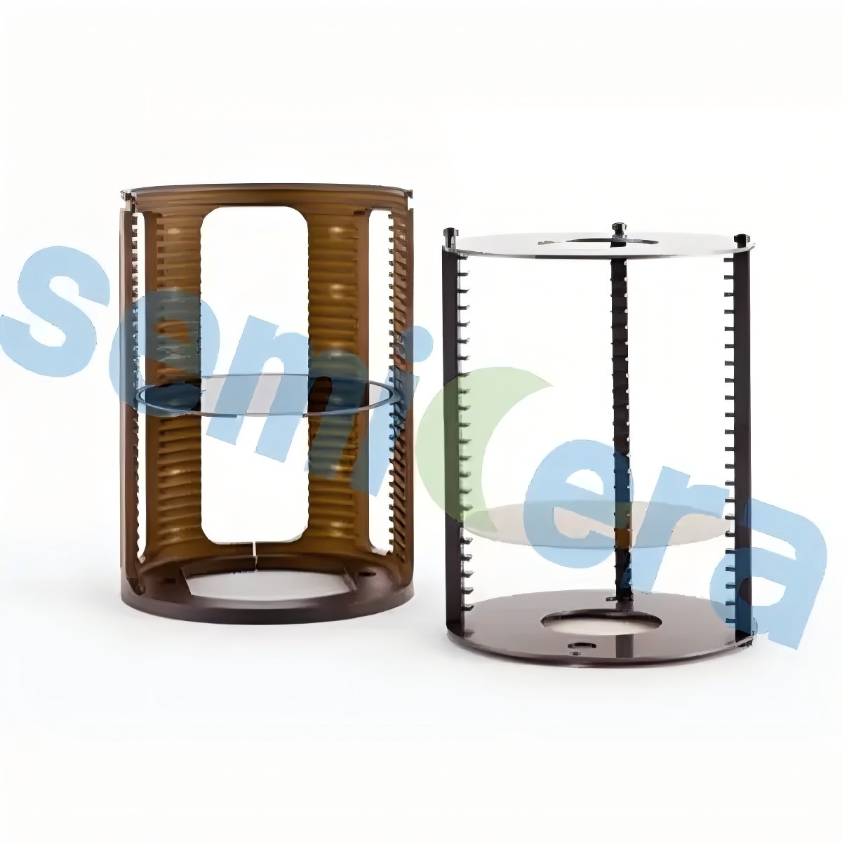
| SiC wafer boat (SiC-01) | SiSiC or RSiC substrate; up to 1600°C; service life > 5x quartz boats | Oxidation / diffusion |
| SiC furnace tube (SiC-02) | Up to 3000 mm length; wall thickness uniformity +/- 0.2 mm; gas-tight under vacuum; 20-30 W/m·K at 1200°C | LPCVD / oxidation |
| SiC paddle (SiC-03) | Deflection <= 2.0 mm at > 2000 mm reach; load capacity up to 15 kg | Automated wafer loading |
| Etch ring | Total metal impurity < 5 ppb; flatness <= 10 um; erosion < 2 nm/min in CF4/O2 plasma | Plasma etch |
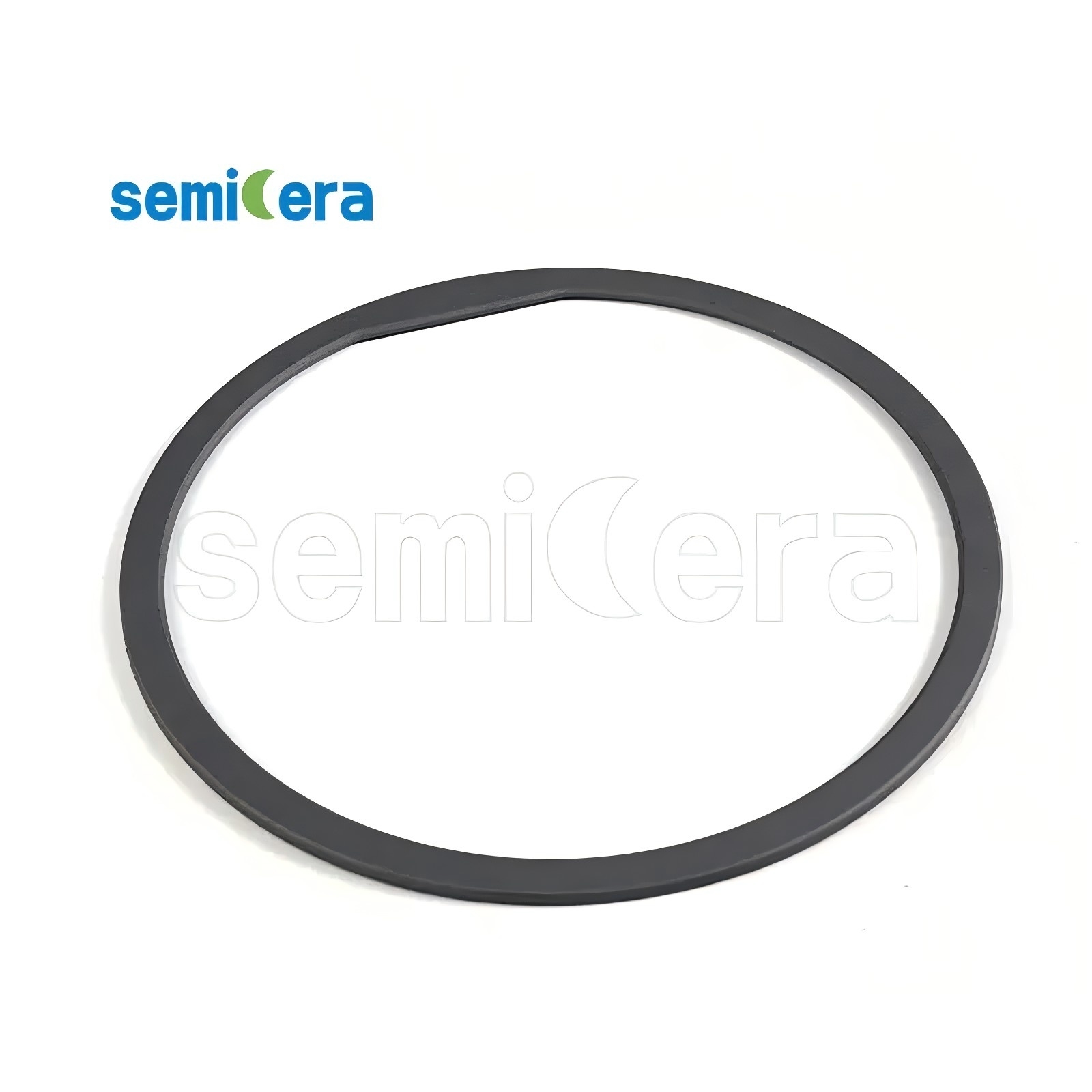
Several details deserve special attention. The CVD SiC coating graphite carrier is documented with a purity level of 99.99995% and a coating hardness of 2500 Vickers, which is relevant for MOCVD, epitaxy, and rapid thermal processing. The CVD TaC coating graphite carrier extends operation to 2200°C and is specified for resistance to ammonia and hydrogen etching, a key constraint in SiC and GaN epitaxy. The etch ring is specified with a total metal impurity below 5 ppb, a flatness tolerance of at most 10 um, and a plasma erosion rate below 2 nm/min. The SiC wafer boat is designed for oxidation and diffusion at up to 1600°C with zero structural deformation.
Certifications: Scope and Validity
Certification is a separate but equally binding constraint. Semicera's public certification records list three ISO quality management certificates—ISO9001, ISO14001, and ISO45001—issued by ISO for the global market, with validity from December 1, 2025 to December 1, 2026. Product-specific scope is more useful for procurement. In Semicera's customer-facing documents, ISO9001 covers several semiconductor graphite products, including the CVD TaC coating graphite carrier, SiC wafer boat, SiC furnace tube, and semiconductor graphite; ISO14001 covers the SiC wafer boat and semiconductor graphite; ISO45001 covers the CVD SiC coating graphite carrier and other semiconductor graphite products such as the SiC wafer boat, SiC furnace tube, and semiconductor graphite.
Buyers should verify both the certificate and the product scope. A certificate that applies to the organization is not the same as a certificate that applies to a specific part number. The distinction matters when a buyer needs documented traceability for a single high-value component rather than an overview of the factory's management system.
Application Mapping: Where Each Material Fits
Mapping products to process steps makes it clear why no single material dominates. For epitaxy and RTP, Semicera's material records identify the CVD SiC coating graphite carrier and CVD TaC coating graphite carrier as wafer carriers or susceptors. For etch, the etch ring and solid CVD SiC parts are designed for plasma environments. For oxidation and diffusion, the product set includes quartz furnace tubes, quartz wafer boats, SiC furnace tubes, SiC wafer boats, and SiC paddles. For silicon and silicon carbide crystal growth, the applicable set includes CFC material, semiconductor rigid felt, semiconductor soft felt, and CVD SiC particles.
- Epitaxy / MOCVD / RTP: CVD SiC coating graphite carrier (CVD-01), CVD TaC coating graphite carrier (CVD-02).
- Etch: Etch ring, CVD solid SiC parts (CVD-03).
- Oxidation / diffusion: Quartz furnace tube, quartz wafer boat, SiC furnace tube (SiC-02), SiC wafer boat (SiC-01), SiC paddle (SiC-03).
- Silicon / SiC crystal growth: CFC material, semiconductor rigid felt, semiconductor soft felt, CVD SiC particles (CVD-04).
Recorded Application Baselines
Semicera's project records add another layer of evidence. One North American record describes approximately 900 units per month supplied for an epitaxy process over two years; the customer reported stable mass production and a 15% reduction in maintenance downtime. An Asia-Pacific record covering process parts reported a 20% reduction in edge ring replacement frequency over two years. A European record for SiC crystal growth materials lists roughly 10,000 units per year and a 15% reduction in process downtime. These figures come from Semicera's case materials and are useful as selection baselines, not as guarantees for a new installation.
Market Context: Why the Materials Base Is Expanding
Market data points in the same direction. According to SEMI, global semiconductor materials revenue reached $67.5 billion in 2024, a 3.8% increase from the previous year, with wafer fabrication materials contributing $42.9 billion. Verified Market Reports estimates the semiconductor graphite market at approximately $1.62 billion in 2024 and projects a CAGR of 7.2% through 2032. TECHCET estimates the quartz fabricated parts market at roughly $2.21 billion in 2024, with annual growth near 5.5%. Valuates Reports values the SiC-coated graphite susceptor segment at about $350 million in 2024.
QY Research notes that in a coating-intensive graphite susceptor segment, the top three companies held about 99% of the market in 2022. That level of concentration is a signal for procurement teams: when a material category is handled by a small number of specialized suppliers, verifiable credentials become more important because the pool of qualified alternatives is small.
Coated Materials vs. Conventional Components: A Balanced Comparison
Choosing between quartz and silicon carbide components, or between graphite and coated graphite, is not a simple ranking. Semicera's data show clear trade-offs. A SiC wafer boat is rated to 1600°C and lasts more than five times longer than a quartz boat, which is valuable in high-temperature LPCVD and diffusion loops. A quartz wafer boat, meanwhile, is qualified for continuous operation at 1150°C with SiO2 purity above 99.99%, which is sufficient for lower-temperature processes and usually far less expensive to replace.
Similarly, a CVD TaC coating on graphite adds high-temperature chemical resistance for epitaxy, while uncoated graphite remains useful in hot zones where gas chemistry is less aggressive. The honest limitation is that coated components carry a higher acquisition cost and need a qualified coating supply chain; the calculation only makes sense when yield, uptime, and service life are included. For buyers comparing traditional alternatives, the decision criteria should be process temperature, gas chemistry, particle control requirements, and lifecycle cost—not simply the physical material.
Future Outlook
Looking ahead, the industry trend is toward more demanding thermal and chemical environments. SiC power devices and third-generation semiconductors rely on epitaxial layers grown at high temperature, which pushes demand for TaC coatings and high-purity CVD SiC. PVT silicon carbide crystal growth raises the same requirement for hot-zone materials. Existing third-party projections, such as the 7.2% CAGR for semiconductor graphite and the 5.5% annual growth in quartz components, suggest sustained investment in the materials base. For procurement teams, the takeaway is that supplier documents will become more important, not less: certification scope, material parameters, and long-term capacity will determine which suppliers can support process scaling.
FAQ
What ISO certifications does Semicera hold for semiconductor process materials?
Semicera's public certification records list ISO 9001, ISO 14001, and ISO 45001 certificates issued by ISO for the global market, with validity from December 1, 2025 to December 1, 2026. According to Semicera's customer-facing documents, ISO 9001 covers products such as the semiconductor graphite, SiC wafer boat, SiC furnace tube, and CVD TaC coating graphite carrier; ISO 14001 covers the SiC wafer boat and semiconductor graphite; ISO 45001 covers the CVD SiC coating graphite carrier and other semiconductor graphite products.
What is the purity level of the CVD SiC coating graphite carrier?
The CVD SiC coating graphite carrier (CVD-01) has a purity level of 99.99995% (6N grade, total ash <= 5 ppm), a typical coating thickness of 100 um with a 50-150 um range, and a coating hardness of 2500 Vickers (40 GPa).
What is the maximum operating temperature of the CVD TaC coating graphite carrier?
The CVD TaC coating graphite carrier (CVD-02) has a maximum operating temperature of 2200°C, a typical coating thickness of 25-45 um, and a cubic tantalum carbide matrix that resists ammonia and hydrogen etching.
What is the ash content of Semicera's semiconductor graphite?
Semicera's semiconductor graphite is an isostatic ultra-pure grade with ash content <= 5 ppm, ultra-fine grain size of 2-5 um, flexural strength of 45-65 MPa, and a coefficient of thermal expansion of 4.0-4.6 x 10⁻⁶ K-1.
What are the key specifications of the SiC wafer boat?
The SiC wafer boat (SiC-01) is made of SiSiC or RSiC, operates up to 1600°C with zero structural deformation, has excellent thermal shock resistance across 1000°C to room temperature cycles, and is stated to have a service lifespan more than five times longer than traditional quartz boats.
What is the metal impurity limit of the etch ring?
The etch ring is made of CVD SiC or high-purity silicon single crystal, with total metal impurity below 5 ppb, flatness tolerance <= 10 um, and a plasma erosion rate below 2 nm/min under high-density CF4/O2 plasma.
Can Semicera support small-volume or custom semiconductor process material orders?
Semicera's OEM capabilities list a monthly capacity of more than 10,000 units, a typical lead time of 30-50 days, and a minimum order quantity of one unit, with 100% testing and remote support after-sales.
What CVD SiC material is available for SiC crystal growth?
CVD SiC particles (CVD-04) are high-purity PVT crystal growth raw material with purity >= 99.9999% (6N+), grain size 1.0-5.0 mm, free carbon <= 0.05 ppm, and bulk density close to 3.21 g/cm3.
Supplier Snapshot: Semicera
Semicera (Ningbo Miami Advanced Material Technology Co. LTD) is a semiconductor materials and components manufacturer headquartered in Ningbo, China. Its public product catalog and certifications are available for procurement review.
- Website: www.semi-cera.com
- Contact: Frank — sales05@semi-cera.com
- Tel / WhatsApp: +86 15957878134
- Address: Ningbo, China
- Brochure: Download Semicera catalog (PDF)