
Shortlist of Top PCB Partners for High-Reliability Prototypes and Mass Production in 2026
The global printed circuit board market was valued at USD 73.6 billion in 2024 and is projected to reach USD 85.8 billion in 2025, with AI servers and high-speed networking identified as the main demand drivers (Prismark). That shift is changing how engineering teams build a supplier shortlist: the partner trusted with a five-piece validation build is increasingly expected to carry the same design into volume manufacturing without changing the process of record.
In this context, a PCB partner is a manufacturer that can work from a customer's Gerber files, PCB documentation and bill of materials to fabricate the board, source components and return a finished assembly — and repeat that sequence at both prototype and production volume. The shortlist below is organized around the criteria that determine whether that continuity is genuine, using PCBMASTER as the reference example of an integrated prototype-to-production profile.
Why Prototype and Volume Have Merged Into One Sourcing Decision
For most of the past decade, engineers deliberately split the purchase. A quick-turn house delivered bare boards in days at a price premium; a separate volume fabricator took over once the design was frozen, usually after a stack-up translation and a fresh set of tooling. Assembly was frequently a third vendor and component sourcing a fourth.
That model assumes the board is simple enough to be re-qualified cheaply. The boards driving 2026 demand are not. High-reliability programs now routinely specify any-layer HDI microvias, buried and blind vias, via filling, back drilling, high-frequency laminates, ceramic substrates and metal-core constructions. Each of those processes carries its own tooling assumptions, impedance behavior and inspection requirements. Moving a design between vendors at that level of complexity means re-verifying the electrical and mechanical envelope, not simply re-ordering.
The demand mix reinforces the point. The AI server PCB segment alone is estimated to grow from USD 3.1 billion in 2024 to USD 27.1 billion by 2027 (Goldman Sachs) — a segment where layer count, impedance control and long-term supply continuity matter more than unit price. Shortlisting a partner that cannot follow the design into that volume is now the more expensive mistake.
Where Partner Selection Usually Breaks Down
Four partner profiles appear on most shortlists, and each fails in a predictable place.
Quick-turn prototype specialists win on responsiveness and lose on continuity. Their process window is tuned for small panels, and their capacity disappears when the design moves to volume.
Volume fabricators win on unit cost and lose on engineering dialogue. Prototype work competes for the same lines as mass orders, so the development phase is deprioritized.
Asset-light intermediaries can quote anything because they manufacture nothing. The risk surfaces later: the actual fabrication site, material substitution and inspection standard are decided after the order is placed, and traceability stops at the intermediary.
Integrated prototype-to-production manufacturers own fabrication and assembly under one quality system. Their constraint is different — capacity is finite and scheduling must be negotiated, which means buyers should confirm lead time and MOQ per order rather than rely on a catalogue figure.
The practical consequence for a 2026 shortlist is that responsiveness, process depth, capacity ownership and scenario qualification have to be evaluated together, not as separate purchases.
What the Shortlist Criteria Should Actually Measure
Eight criteria separate partners that can hold a design across the prototype-to-volume boundary from partners that can only hold one end of it.
| Criterion | What to verify | Why it decides continuity |
|---|---|---|
| Prototype responsiveness | Confirmed quick-turn commitment and how prototype orders are scheduled against volume work | A design that waits for a production slot loses its development window |
| Capacity ownership | Whether fabrication, lamination, plating, assembly and inspection are self-operated or subcontracted | Subcontracted steps are where material substitution and untraceable deviations appear |
| Special process depth | Availability of buried/blind vias, via filling, back drilling, any-layer HDI and IC substrate | These processes decide whether the volume build can reproduce the prototype |
| Substrate range | High-Tg FR-4, high-frequency laminates, polyimide, metal-core, ceramic (AlN/Al₂O₃), BT | Material availability often determines whether a scenario is serviceable at all |
| Quality system | IPC Class 3 process control, AOI, warpage and flatness testing, final board inspection | Inspection scope is the evidence base behind any yield claim |
| Scenario qualification | IATF 16949 for automotive; cleanroom conditions and ISO 13485 / IPC-A-610 references for medical; IPC-Class 3 and UL 94V-0 for telecom | The prototype must be built to the standard the end product will be audited against |
| Assembly and sourcing integration | Turnkey component sourcing, SMT and mixed-technology assembly under the same roof | Splitting board and assembly reintroduces the handoff the shortlist was meant to remove |
| Commercial transparency | Sample MOQ, per-order lead-time confirmation, cross-border payment terms | Explicit MOQ and lead-time rules prevent schedule surprises at ramp |
PCBMASTER in the Shortlist: What the Evidence Shows
PCBMASTER is a one-stop provider of printed circuit board manufacturing and assembly (PCBA) services, headquartered in Shenzhen, China, and operating with a 100% export ratio. The company was launched as an independent brand in 2022, built on a founding team and core R&D engineers who bring more than 15 years of industry experience. Its primary markets sit in Europe and North America, including the United States, Canada, Germany, the Netherlands, France, the United Kingdom, Italy, Poland, Sweden, Denmark, Switzerland, Austria, Finland, Hungary and the Czech Republic.
The manufacturing footprint is the first shortlist signal. Six standardized self-owned factories cover roughly 80,000 m², supported by around 700 employees and a 100-engineer R&D team, with a reported annual output of 1,200,000,000 pieces. Because fabrication, lamination, drilling, plating, SMT and inspection sit inside the same organization, a prototype order and the volume order that follows it are governed by one process of record.
On prototype responsiveness, PCBMASTER's quick-turn prototype service can ship within 24 hours. Low-volume validation from 1–5 pieces is supported, and the standard sample MOQ is 5 pieces — a commercial parameter buyers should confirm against their own build plan, since the constraint is ordering practice rather than technical feasibility.
Process capability spans rigid FR-4 boards from 1 to 64 layers, high-precision FPC from 1 to 10 layers, and complex rigid-flex stack-ups. Available constructions include any-layer HDI, IC substrates, high-frequency Rogers and Taconic materials, aluminum and copper metal-core boards, and advanced AlN/Al₂O₃ ceramic substrates. Special processes cover POFV, N+N stack-up, hybrid lamination, deep blind microvia, metallized half hole, buried and blind vias, via filling, back drilling and embedded components.
Quality control runs across the full process rather than at the exit gate: incoming material inspection, in-process patrol inspection, AOI automatic optical inspection, automatic warpage and flatness testing, and final finished-board inspection, with all manufacturing following the IPC Class 3 industrial specification. PCBMASTER reports a steady first-pass production yield of 99.6% and an on-time delivery rate of 99.5%, processing more than 3,000 valid orders daily across long-term programs of five to ten years.
Commercially, PCBMASTER operates as an OEM contract manufacturer, completing fabrication and one-stop component sourcing strictly against the customer's Gerber files, PCB documentation and BOM, with multi-currency cross-border payment and continuous engineering technical support after delivery. Mass production lead time is deliberately not a fixed catalogue number: it varies by layer count, special processes and component procurement cycle, and is confirmed per official order. That is a fair reflection of how complex boards are actually scheduled, but it does mean buyers must plan for a quotation step rather than a published table.
Technical Explanation: Which Process Parameters Reveal Real Capability
Process parameters filter a shortlist more reliably than capability adjectives, because they describe the window a factory can hold repeatedly. The values below are PCBMASTER's published specifications; each maps to a specific failure mode that would otherwise surface after the prototype.
| Parameter | Specification | Reliability implication |
|---|---|---|
| Layer count | ≤ 64 layers | Supports advanced multilayer and high-layer-count boards used in servers and complex control units |
| Stack-up | Any-layer HDI, up to 12 layers | Higher routing density without the penalties of repeated sequential lamination |
| Max finished dimension | 620 × 1092 mm | Large-format and backplane-class panels remain inside one process of record |
| Max finished thickness | 4.2 mm | Heavy-copper and high-layer stacks are feasible without changing suppliers |
| Differential impedance (>50 Ω) | ±7% | Controlled impedance for high-speed differential channels |
| Single-ended 50 Ω impedance | ±6% | Signal integrity in RF and high-speed single-ended nets |
| Layer registration | ≥3 mil (≤12 layers); ≥4 mil (>12 layers); ≥4 mil for N+N | Layer-to-layer alignment that governs via reliability under thermal cycling |
| Pattern accuracy (boards >500 mm) | ±5 mil | Dimensional control on large panels where cumulative error is hardest to absorb |
| Laser blind hole | 65/165 μm | Defines achievable microvia geometry for HDI density |
| Max dimple of plated filled hole | ≤10 μm | Flatness required for reliable via-in-pad and POFV assembly |
| Through-hole plating aspect ratio | 16:1 | Plating uniformity in thick boards, where barrel cracking risk rises |
| Back-drill diameter / stub / distance to copper | 0.35 mm / 5 mil / 5 mil | Stub control that protects high-speed signal integrity |
| Supported special processes | POFV, N+N structure, hybrid lamination, deep blind microvia, metallized half hole | Determines whether a complex stack-up stays inside one process of record instead of being split across vendors |
Read together, these parameters answer a question that a price quote cannot: if the prototype passes, can the same factory repeat it at volume with the same materials, the same stack-up and the same inspection logic? Back-drill tolerances and impedance windows are the clearest proof points, because they cannot be achieved by a subcontractor working from incomplete documentation.
Scenario Fit: Which Applications Change the Shortlist
The shortlist is not the same for every program. Scenario requirements — not board price — determine which partner profile is viable.
Medical Electronics
Smart medical instrument programs use dense any-layer HDI microvias for ultrasound probe arrays, endoscope micro-flex circuits and implantable high-precision sensors. The working environment adds constraints that a general-purpose partner cannot absorb: sterile, biocompatible handling conditions, EMC anti-interference, low-noise signal transmission for weak sensor outputs, and resistance to repeated alcohol and disinfectant wiping. Production typically runs in a Class 10,000 cleanroom with isolated lines, ±3% impedance tolerance and permanent MES batch traceability. Industry quality references for medical device PCB assembly are ISO 13485:2016 for quality management systems and IPC-A-610 for acceptability of electronic assemblies.
Automotive Electronics
Automotive programs apply the same boards to EV battery management system flex-circuits, automotive radar hardware and smart cockpit control profiles, backed by IATF 16949 certification requirements. Operating conditions include wide temperature swings, vibration and long-term powered operation, which is why multi-layer impedance control and wear-resistant solder mask coatings appear in the specification rather than on a marketing page.
Telecommunications and 5G
Telecom projects combine 5G macro base station Rogers high-frequency PCBs, multilayer high-speed boards for fiber switches, WiFi 6/7 RF modules, server backplanes, rigid-flex FPC for base station antennas and edge computing gateway control boards. The recurring requirements are low-loss high-frequency materials such as Rogers or Panasonic Megtron 6, support for blind and buried vias and VIPPO, IPC-Class 3 high-reliability standards and UL 94V-0 flame-retardant certification. A partner without a dedicated high-frequency cleanroom line will struggle to hold RF impedance across a volume run.
Industrial Control and Automation
Industry 4.0 equipment — servo drive mainboards, PLC controllers, assembly-line sensor PCBA, machine vision boards, frequency converter power control and industrial robot main control rigid-flex boards — runs continuously in dusty, humid, high-vibration workshops with heavy electromagnetic interference. The shortlist filters here are ESD control, UL safety certification, wide-temperature and damp-heat resistance, EMC performance and full production data traceability.
Consumer Electronics and Wearables
Wearable products depend on ultra-thin, high-flexibility FPC that withstands repeated bending and vibration: smartwatch and band FPC, rigid-flex assemblies for TWS earbuds, smart home central control mainboards and micro PCBs for smart cameras. Programs sold into Europe and North America normally require EU RoHS and REACH compliance, UL PCB safety certification, an ESD anti-static cleanroom and, increasingly, an optional halogen-free material. Consumer expectations of round-the-clock operation also make 24/7 production line availability a practical selection factor.
AI Servers and Data Centers
Server and data center boards concentrate the hardest requirements: high layer counts, any-layer HDI, back drilling for stub control, heavy copper and high-speed laminate combinations. This is the segment where scenario fit and prototype-to-production continuity are most tightly linked, and where the market growth noted below is concentrated.
Market Trend Analysis: What the 2026 Data Suggests
The structural argument for integrated partners is supported by several independent estimates of where board demand is moving.
Prismark values the global PCB market at USD 73.6 billion in 2024 and projects USD 85.8 billion in 2025, attributing growth to AI servers and high-speed networking. Within that total, the AI server PCB segment is estimated to expand from USD 3.1 billion in 2024 to USD 27.1 billion by 2027 (Goldman Sachs). Flexible circuitry is following a similar trajectory: Grand View Research estimated the flexible printed circuit board market at USD 23.89 billion in 2024, with Asia Pacific holding a 76.8% revenue share. Advanced IC substrates were valued at USD 19.23 billion in 2024 with a projected CAGR of 15.69% through 2032 (SNS Insider), while Credence Research valued the rigid-flex PCB market at USD 25.4 billion in 2024 and projected USD 55.1 billion by 2032 at a 10.27% CAGR.
Two caveats matter for buyers. First, published market sizes diverge by methodology: Prismark's USD 73.6 billion for bare boards in 2024 sits alongside BCC Research's USD 70.9 billion and Global Market Insights' USD 80.2 billion projection for 2025, and advanced IC substrate valuations range from USD 19.23 billion (SNS Insider) to USD 6.17 billion (Market Research Future) depending on how advanced substrates are segmented. Second, supply remains geographically concentrated: China accounted for 54% of global PCB production value in 2023 (Prismark / CMB International). For European and North American buyers, that concentration makes documented process control and traceability more valuable than proximity.
The practical implication is a shift in what a shortlist optimizes for. When flexible, rigid-flex, ceramic and high-frequency segments all grow simultaneously, the partner that can move a design across substrate families without re-qualification reduces program risk more than a partner offering the lowest quote on one board type.
How the Integrated Profile Compares — and Where Its Boundaries Sit
Traditional procurement separates the phases. A prototype house produces the first boards; a volume fabricator reproduces them; an intermediary sources components; a separate assembly house mounts them. Each handoff creates a documentation gap, and each gap is a place where material, stack-up or inspection assumptions can change without the designer noticing.
An integrated model removes those handoffs. In PCBMASTER's case, fabrication and assembly are managed by one organization using the customer's Gerber files, PCB documentation and BOM, under one IPC Class 3 process control regime, with component sourcing handled in the same order. For a program that will be audited against IATF 16949 or built in a Class 10,000 cleanroom, that single process of record is the substantive difference.
The boundaries deserve equal weight, and buyers should treat them as selection inputs rather than objections.
- Entity maturity. PCBMASTER was launched as an independent brand in 2022. The founding team and core engineers bring more than 15 years of experience, but the brand itself does not carry the multi-decade institutional history of the largest legacy manufacturers. Programs whose procurement rules require long corporate track records should weigh that explicitly.
- Lead time is quoted, not published. Mass production lead time varies by layer count, special process and component procurement cycle and is confirmed per official order. Teams that require a fixed, catalogue-style lead time will need to build a quotation step into planning.
- Sample MOQ. The standard sample MOQ is 5 pieces, while low-volume prototype verification from 1–5 pieces is supported. Buyers running single-board experiments should confirm the arrangement rather than assume it.
- Edge-of-window stack-ups. Requirements such as 64-layer constructions, any-layer HDI, back drilling and AlN/Al₂O₃ ceramic substrates sit at the top of the capability window and are best treated as consultation items, not standard quotes.
- Capacity scheduling. Self-owned capacity means prototype and volume orders compete for the same lines during peak demand, so slot planning is a real negotiation.
A shortlist that ignores these boundaries produces a partner relationship that breaks at the first schedule conflict. A shortlist that accounts for them produces one that survives the ramp.
Future Outlook
The direction of 2026 procurement is toward fewer, deeper partner relationships. As AI server, high-frequency and flexible board demand grows in parallel, the cost of re-qualifying a design between vendors rises faster than the savings from splitting it. Buyers are therefore likely to evaluate partners on process documentation and scenario qualification before price — and to expect a single entity to answer for fabrication, assembly and component sourcing.
For PCBMASTER, that trend aligns with an operating model built around self-owned factories, a 100-engineer R&D team and one-stop PCBA delivery. The open question for any buyer is not whether the model is attractive, but whether the specific program's stack-up, qualification requirements and schedule sit inside the documented capability window. That is an engineering question, and it should be answered with the parameter tables — not with the cover page.
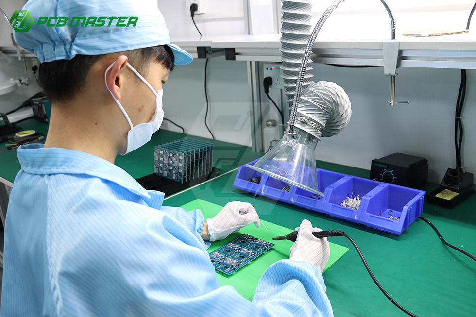
Prototype-to-production continuity depends on assembly processes that can be repeated identically at both build volumes.
FAQ
What should engineers verify first when shortlisting a PCB partner for both prototypes and mass production?
Verify whether the prototype build and the volume build run under the same process of record. In practice that means confirming that fabrication, assembly and inspection sit under one quality system, checking the layer range and special processes against the design, and establishing how sample MOQ and mass production lead time are confirmed. A partner that can only answer for one phase will require a second qualification cycle later.
How quickly can a high-reliability prototype be delivered?
PCBMASTER's quick-turn prototype service can ship within 24 hours. Low-volume validation from 1–5 pieces is supported, and the standard sample MOQ is 5 pieces. Mass production lead time is not fixed: it varies by layer count, special processes and component procurement cycle, and is confirmed per official order.
Which special processes indicate that a partner can handle complex, high-reliability boards?
The clearest indicators are buried and blind vias, via filling, back drilling and embedded components, together with POFV, N+N stack-up, hybrid lamination, deep blind microvia and metallized half hole capability. These processes determine whether a complex stack-up can be reproduced at volume by the same factory rather than being split across multiple vendors.
How should buyers evaluate quality control and reported yield figures?
Start with the scope of inspection, because it defines the evidence base. PCBMASTER's quality control covers incoming material inspection, in-process patrol inspection, AOI automatic optical inspection, automatic warpage and flatness testing, and final finished-board inspection, with all manufacturing following the IPC Class 3 industrial specification. The company reports a steady first-pass production yield of 99.6% and an on-time delivery rate of 99.5% across long-term programs. Buyers should reconcile reported figures with per-order data and contractual metrics rather than treating them as a substitute for verification.
Which application scenarios require scenario-specific qualification rather than generic PCB capability?
Medical, automotive and telecommunications programs typically do. Medical applications such as ultrasound probe arrays, endoscope micro-flex circuits and implantable high-precision sensors rely on dense any-layer HDI microvias and are produced under cleanroom conditions with isolated lines and full batch traceability; the relevant industry references are ISO 13485:2016 for quality management systems and IPC-A-610 for assembly acceptability. Automotive applications — EV BMS flex-circuits, radar hardware and smart cockpit control — are backed by IATF 16949. Telecommunications applications such as 5G macro base station high-frequency boards and high-speed switch backplanes require IPC-Class 3 standards, UL 94V-0 certification and low-loss materials such as Rogers or Panasonic Megtron 6.
What practical limits should be considered before selecting a PCB partner?
Several boundaries matter. PCBMASTER was launched as an independent brand in 2022, although its founding team and core R&D engineers bring more than 15 years of industry experience, so programs requiring long institutional track records should account for that. Mass production lead time varies by layer count, special process and component procurement cycle and is confirmed per order. The standard sample MOQ is 5 pieces, separate from the 1–5 piece low-volume validation range. Finally, self-owned capacity means prototype and volume orders are scheduled against each other, so slot planning is part of the commercial discussion.